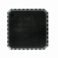
ATMEGA8L-8MU Atmel, ATMEGA8L-8MU Datasheet - Page 73

ATMEGA8L-8MU
Manufacturer Part Number
ATMEGA8L-8MU
Description
IC AVR MCU 8K 8MHZ 3V 32-QFN
Manufacturer
Atmel
Series
AVR® ATmegar
Specifications of ATMEGA8L-8MU
Core Processor
AVR
Core Size
8-Bit
Speed
8MHz
Connectivity
I²C, SPI, UART/USART
Peripherals
Brown-out Detect/Reset, POR, PWM, WDT
Number Of I /o
23
Program Memory Size
8KB (4K x 16)
Program Memory Type
FLASH
Eeprom Size
512 x 8
Ram Size
1K x 8
Voltage - Supply (vcc/vdd)
2.7 V ~ 5.5 V
Data Converters
A/D 8x10b
Oscillator Type
Internal
Operating Temperature
-40°C ~ 85°C
Package / Case
32-VQFN Exposed Pad, 32-HVQFN, 32-SQFN, 32-DHVQFN
Package
32MLF EP
Device Core
AVR
Family Name
ATmega
Maximum Speed
8 MHz
Operating Supply Voltage
3.3|5 V
Data Bus Width
8 Bit
Number Of Programmable I/os
23
Interface Type
SPI/TWI/USART
On-chip Adc
8-chx10-bit
Number Of Timers
3
Controller Family/series
AVR MEGA
No. Of I/o's
23
Eeprom Memory Size
512Byte
Ram Memory Size
1KB
Cpu Speed
8MHz
Rohs Compliant
Yes
For Use With
ATSTK600-TQFP32 - STK600 SOCKET/ADAPTER 32-TQFPATSTK600-DIP40 - STK600 SOCKET/ADAPTER 40-PDIP770-1007 - ISP 4PORT ATMEL AVR MCU SPI/JTAGATAVRISP2 - PROGRAMMER AVR IN SYSTEMATSTK500 - PROGRAMMER AVR STARTER KIT
Lead Free Status / RoHS Status
Lead free / RoHS Compliant
Available stocks
Company
Part Number
Manufacturer
Quantity
Price
Part Number:
ATMEGA8L-8MU
Manufacturer:
AT
Quantity:
20 000
- Current page: 73 of 302
- Download datasheet (6Mb)
Timer/Counter0
and
Timer/Counter1
Prescalers
Internal Clock Source
Prescaler Reset
External Clock Source
2486Z–AVR–02/11
Timer/Counter1 and Timer/Counter0 share the same prescaler module, but the Timer/Counters
can have different prescaler settings. The description below applies to both Timer/Counter1 and
Timer/Counter0.
The Timer/Counter can be clocked directly by the system clock (by setting the CSn2:0 = 1). This
provides the fastest operation, with a maximum Timer/Counter clock frequency equal to system
clock frequency (f
clock source. The prescaled clock has a frequency of either f
f
The prescaler is free running (that is, operates independently of the clock select logic of the
Timer/Counter) and it is shared by Timer/Counter1 and Timer/Counter0. Since the prescaler is
not affected by the Timer/Counter’s clock select, the state of the prescaler will have implications
for situations where a prescaled clock is used. One example of prescaling artifacts occurs when
the timer is enabled and clocked by the prescaler (6 > CSn2:0 > 1). The number of system clock
cycles from when the timer is enabled to the first count occurs can be from 1 to N+1 system
clock cycles, where N equals the prescaler divisor (8, 64, 256, or 1024).
It is possible to use the prescaler reset for synchronizing the Timer/Counter to program execu-
tion. However, care must be taken if the other Timer/Counter that shares the same prescaler
also uses prescaling. A prescaler reset will affect the prescaler period for all Timer/Counters it is
connected to.
An external clock source applied to the T1/T0 pin can be used as Timer/Counter clock
(clk
logic. The synchronized (sampled) signal is then passed through the edge detector.
shows a functional equivalent block diagram of the T1/T0 synchronization and edge detector
logic. The registers are clocked at the positive edge of the internal system clock (
is transparent in the high period of the internal system clock.
The edge detector generates one clk
(CSn2:0 = 6) edge it detects.
Figure 30. T1/T0 Pin Sampling
The synchronization and edge detector logic introduces a delay of 2.5 to 3.5 system clock cycles
from an edge has been applied to the T1/T0 pin to the counter is updated.
Enabling and disabling of the clock input must be done when T1/T0 has been stable for at least
one system clock cycle, otherwise it is a risk that a false Timer/Counter clock pulse is generated.
Each half period of the external clock applied must be longer than one system clock cycle to
ensure correct sampling. The external clock must be guaranteed to have less than half the sys-
tem clock frequency (f
CLK_I/O
T1
/clk
clk
Tn
/1024.
I/O
T0
). The T1/T0 pin is sampled once every system clock cycle by the pin synchronization
D Q
LE
CLK_I/O
Synchronization
ExtClk
). Alternatively, one of four taps from the prescaler can be used as a
D Q
< f
clk_I/O
/2) given a 50/50% duty cycle. Since the edge detector uses
T1
/clk
T
0
pulse for each positive (CSn2:0 = 7) or negative
D Q
CLK_I/O
Edge Detector
/8, f
CLK_I/O
ATmega8(L)
/64, f
Tn_sync
(To Clock
Select Logic)
clk
CLK_I/O
I/O
). The latch
Figure 30
/256, or
73
Related parts for ATMEGA8L-8MU
Image
Part Number
Description
Manufacturer
Datasheet
Request
R

Part Number:
Description:
8-bit AVR with 8K Bytes In-System Programmable Flash
Manufacturer:
ATMEL [ATMEL Corporation]
Datasheet:

Part Number:
Description:
IC AVR MCU 8K 8MHZ 3V 28DIP
Manufacturer:
Atmel
Datasheet:

Part Number:
Description:
IC AVR MCU 8K LV 8MHZ COM 32TQFP
Manufacturer:
Atmel
Datasheet:

Part Number:
Description:
IC AVR MCU 8K LV 8MHZ IND 32TQFP
Manufacturer:
Atmel
Datasheet:

Part Number:
Description:
IC AVR MCU 8K LV 8MHZ COM 28-DIP
Manufacturer:
Atmel
Datasheet:

Part Number:
Description:
IC AVR MCU 8K LV 8MHZ IND 28-DIP
Manufacturer:
Atmel
Datasheet:

Part Number:
Description:
IC AVR MCU 8K LV 8MHZ COM 32-QFN
Manufacturer:
Atmel
Datasheet:

Part Number:
Description:
IC AVR MCU 8K LV 8MHZ IND 32-QFN
Manufacturer:
Atmel
Datasheet:

Part Number:
Description:
MCU AVR 8KB FLASH 8MHZ 32TQFP
Manufacturer:
Atmel
Datasheet:

Part Number:
Description:
MCU AVR 8KB FLASH 8MHZ 32QFN
Manufacturer:
Atmel
Datasheet:

Part Number:
Description:
IC MCU AVR 8K 5V 8MHZ 32-TQFP
Manufacturer:
Atmel
Datasheet:

Part Number:
Description:
IC MCU AVR 8K 5V 8MHZ 32-QFN
Manufacturer:
Atmel
Datasheet:

Part Number:
Description:
IC MCU AVR 8K 5V 8MHZ 28-DIP
Manufacturer:
Atmel
Datasheet:


