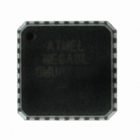
ATMEGA8L-8MU Atmel, ATMEGA8L-8MU Datasheet - Page 114

ATMEGA8L-8MU
Manufacturer Part Number
ATMEGA8L-8MU
Description
IC AVR MCU 8K 8MHZ 3V 32-QFN
Manufacturer
Atmel
Series
AVR® ATmegar
Specifications of ATMEGA8L-8MU
Core Processor
AVR
Core Size
8-Bit
Speed
8MHz
Connectivity
I²C, SPI, UART/USART
Peripherals
Brown-out Detect/Reset, POR, PWM, WDT
Number Of I /o
23
Program Memory Size
8KB (4K x 16)
Program Memory Type
FLASH
Eeprom Size
512 x 8
Ram Size
1K x 8
Voltage - Supply (vcc/vdd)
2.7 V ~ 5.5 V
Data Converters
A/D 8x10b
Oscillator Type
Internal
Operating Temperature
-40°C ~ 85°C
Package / Case
32-VQFN Exposed Pad, 32-HVQFN, 32-SQFN, 32-DHVQFN
Package
32MLF EP
Device Core
AVR
Family Name
ATmega
Maximum Speed
8 MHz
Operating Supply Voltage
3.3|5 V
Data Bus Width
8 Bit
Number Of Programmable I/os
23
Interface Type
SPI/TWI/USART
On-chip Adc
8-chx10-bit
Number Of Timers
3
Controller Family/series
AVR MEGA
No. Of I/o's
23
Eeprom Memory Size
512Byte
Ram Memory Size
1KB
Cpu Speed
8MHz
Rohs Compliant
Yes
For Use With
ATSTK600-TQFP32 - STK600 SOCKET/ADAPTER 32-TQFPATSTK600-DIP40 - STK600 SOCKET/ADAPTER 40-PDIP770-1007 - ISP 4PORT ATMEL AVR MCU SPI/JTAGATAVRISP2 - PROGRAMMER AVR IN SYSTEMATSTK500 - PROGRAMMER AVR STARTER KIT
Lead Free Status / RoHS Status
Lead free / RoHS Compliant
Available stocks
Company
Part Number
Manufacturer
Quantity
Price
Part Number:
ATMEGA8L-8MU
Manufacturer:
AT
Quantity:
20 000
- Current page: 114 of 302
- Download datasheet (6Mb)
8-bit
Timer/Counter
Register
Description
Timer/Counter Control
Register – TCCR2
114
ATmega8(L)
Figure 55
Figure 55. Timer/Counter Timing Diagram, Clear Timer on Compare Match Mode, with Pres-
caler (f
• Bit 7 – FOC2: Force Output Compare
The FOC2 bit is only active when the WGM bits specify a non-PWM mode. However, for ensur-
ing compatibility with future devices, this bit must be set to zero when TCCR2 is written when
operating in PWM mode. When writing a logical one to the FOC2 bit, an immediate Compare
Match is forced on the waveform generation unit. The OC2 output is changed according to its
COM21:0 bits setting. Note that the FOC2 bit is implemented as a strobe. Therefore it is the
value present in the COM21:0 bits that determines the effect of the forced compare.
A FOC2 strobe will not generate any interrupt, nor will it clear the timer in CTC mode using
OCR2 as TOP.
The FOC2 bit is always read as zero.
• Bit 6:3 – WGM21:0: Waveform Generation Mode
These bits control the counting sequence of the counter, the source for the maximum (TOP)
counter value, and what type of waveform generation to be used. Modes of operation supported
by the Timer/Counter unit are: Normal mode, Clear Timer on Compare Match (CTC) mode, and
two types of Pulse Width Modulation (PWM) modes. See
Operation” on page
Bit
Read/Write
Initial Value
TCNTn
(clk
OCRn
(CTC)
OCFn
clk
clk
clk_I/O
I/O
I/O
Tn
shows the setting of OCF2 and the clearing of TCNT2 in CTC mode.
/8)
/8)
FOC2
W
7
0
108.
WGM20
R/W
TOP - 1
6
0
COM21
R/W
5
0
COM20
R/W
0
4
TOP
WGM21
R/W
3
0
TOP
CS22
R/W
2
0
Table 42 on page 115
BOTTOM
CS21
R/W
1
0
CS20
R/W
0
0
BOTTOM + 1
TCCR2
and
2486Z–AVR–02/11
“Modes of
Related parts for ATMEGA8L-8MU
Image
Part Number
Description
Manufacturer
Datasheet
Request
R

Part Number:
Description:
8-bit AVR with 8K Bytes In-System Programmable Flash
Manufacturer:
ATMEL [ATMEL Corporation]
Datasheet:

Part Number:
Description:
IC AVR MCU 8K 8MHZ 3V 28DIP
Manufacturer:
Atmel
Datasheet:

Part Number:
Description:
IC AVR MCU 8K LV 8MHZ COM 32TQFP
Manufacturer:
Atmel
Datasheet:

Part Number:
Description:
IC AVR MCU 8K LV 8MHZ IND 32TQFP
Manufacturer:
Atmel
Datasheet:

Part Number:
Description:
IC AVR MCU 8K LV 8MHZ COM 28-DIP
Manufacturer:
Atmel
Datasheet:

Part Number:
Description:
IC AVR MCU 8K LV 8MHZ IND 28-DIP
Manufacturer:
Atmel
Datasheet:

Part Number:
Description:
IC AVR MCU 8K LV 8MHZ COM 32-QFN
Manufacturer:
Atmel
Datasheet:

Part Number:
Description:
IC AVR MCU 8K LV 8MHZ IND 32-QFN
Manufacturer:
Atmel
Datasheet:

Part Number:
Description:
MCU AVR 8KB FLASH 8MHZ 32TQFP
Manufacturer:
Atmel
Datasheet:

Part Number:
Description:
MCU AVR 8KB FLASH 8MHZ 32QFN
Manufacturer:
Atmel
Datasheet:

Part Number:
Description:
IC MCU AVR 8K 5V 8MHZ 32-TQFP
Manufacturer:
Atmel
Datasheet:

Part Number:
Description:
IC MCU AVR 8K 5V 8MHZ 32-QFN
Manufacturer:
Atmel
Datasheet:

Part Number:
Description:
IC MCU AVR 8K 5V 8MHZ 28-DIP
Manufacturer:
Atmel
Datasheet:


