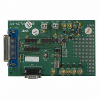
EVAL-AD7706EB Analog Devices Inc, EVAL-AD7706EB Datasheet - Page 6
EVAL-AD7706EB
Manufacturer Part Number
EVAL-AD7706EB
Description
BOARD EVAL FOR AD7706
Manufacturer
Analog Devices Inc
Datasheet
1.EVAL-AD7705EB.pdf
(32 pages)
Specifications of EVAL-AD7706EB
Number Of Adc's
1
Number Of Bits
16
Sampling Rate (per Second)
500
Data Interface
Serial
Inputs Per Adc
3 Differential
Input Range
0 ~ 5.25 V
Power (typ) @ Conditions
6.5mW @ 500SPS
Voltage Supply Source
Single
Operating Temperature
-40°C ~ 85°C
Utilized Ic / Part
AD7706
Lead Free Status / RoHS Status
Contains lead / RoHS non-compliant


AD7705/AD7706
Pin No.
1
2
3
4
5
6
7
8
9
Mnemonic
SCLK
MCLK IN
MCLK OUT
CS
RESET
AIN2(+)[AIN1]
AIN1(+)[AIN2]
AIN1(–)[COMMON]
REF IN(+)
MCLK OUT
MCLK IN
AIN2(+)
AIN1(+)
AIN1(–)
RESET
SCLK
CS
1
2
3
4
5
6
7
8
(Not to Scale)
TOP VIEW
AD7705
AD7705: Positive input of the differential Analog Input Channel 2. AD7706: Analog Input
AD7705: Positive input of the differential Analog Input Channel 1. AD7706: Analog Input
AD7705: Negative input of the differential Analog Input Channel 1. AD7706: COMMON
Function
Serial Clock. Schmitt-Triggered Logic Input. An external serial clock is applied to this input
to access serial data from the AD7705/AD7706. This serial clock can be a continuous clock
with all data transmitted in a continuous train of pulses. Alternatively, it can be a noncon-
tinuous clock with the information being transmitted to the AD7705/AD7706 in smaller
batches of data.
Master Clock signal for the device. This can be provided in the form of a crystal/resonator or
external clock. A crystal/resonator can be tied across the MCLK IN and MCLK OUT pins.
Alternatively, the MCLK IN pin can be driven with a CMOS-compatible clock and MCLK
OUT left unconnected. The part can be operated with clock frequencies in the range
500 kHz to 5 MHz.
When the master clock for the device is a crystal/resonator, the crystal/resonator is connected
between MCLK IN and MCLK OUT. If an external clock is applied to MCLK IN, MCLK
OUT provides an inverted clock signal. This clock can be used to provide a clock source for
external circuitry and is capable of driving one CMOS load. If the user does not require it,
this MCLK OUT can be turned off via the CLK DIS bit of the Clock Register. This ensures
that the part is not burning unnecessary power driving capacitive loads on MCLK OUT.
Chip Select. Active low Logic Input used to select the AD7705/AD7706. With this input
hard-wired low, the AD7705/AD7706 can operate in its three-wire interface mode with
SCLK, DIN and DOUT used to interface to the device. CS can be used to select the device
in systems with more than one device on the serial bus or as a frame synchronization signal in
communicating with the AD7705/AD7706.
Logic Input. Active low input that resets the control logic, interface logic, calibration
coefficients, digital filter and analog modulator of the part to power-on status.
Channel 1.
Channel 2.
Input. Analog inputs for Channels 1, 2 and 3 are referenced to this input.
Reference Input. Positive input of the differential Reference Input to the AD7705/AD7706.
The reference input is differential with the provision that REF IN(+) must be greater than
REF IN(–). REF IN(+) can lie anywhere between V
16
15
14
13
12
11
10
9
GND
V
DIN
DOUT
DRDY
AIN2(–)
REF IN(–)
REF IN(+)
DD
PIN FUNCTION DESCRIPTIONS
PIN CONFIGURATIONS
–6–
MCLK OUT
COMMON
MCLK IN
RESET
SCLK
AIN1
AIN2
CS
1
2
3
4
5
6
7
8
DD
(Not to Scale)
TOP VIEW
and GND.
AD7706
16
15
14
13
12
11
10
9
GND
V
DIN
DOUT
DRDY
AIN3
REF IN(–)
REF IN(+)
DD
REV. A
Related parts for EVAL-AD7706EB
Image
Part Number
Description
Manufacturer
Datasheet
Request
R

Part Number:
Description:
ENERCHIP CC EVAL KIT
Manufacturer:
Cymbet Corporation
Datasheet:

Part Number:
Description:
BOARD EVAL FOR AD976
Manufacturer:
Analog Devices Inc
Datasheet:

Part Number:
Description:
BOARD EVAL FOR ADXL345
Manufacturer:
Analog Devices Inc
Datasheet:

Part Number:
Description:
ENERCHIP CC SEH EVAL KIT
Manufacturer:
Cymbet Corporation
Datasheet:

Part Number:
Description:
ENERCHIP EP ENERGY HARVEST EVAL
Manufacturer:
Cymbet Corporation
Datasheet:

Part Number:
Description:
EVAL BOARD FOR TW6864-LB2-GR
Manufacturer:
Intersil
Datasheet:
Part Number:
Description:
EVAL BOARD FOR TW8816-LB3-GR
Manufacturer:
Intersil
Datasheet:
Part Number:
Description:
EVAL BOARD FOR TW8817-TA3-GRS
Manufacturer:
Intersil
Datasheet:

Part Number:
Description:
EVALUATION MODULE FOR ADUM4160
Manufacturer:
Analog Devices Inc
Datasheet:

Part Number:
Description:
BOARD EVALUATION ADCMP581BCP
Manufacturer:
Analog Devices Inc
Datasheet:
Part Number:
Description:
BOARD EVALUATION ADM1041
Manufacturer:
Analog Devices Inc
Datasheet:

Part Number:
Description:
EVAL BOARD FOR STM32F107VCT
Manufacturer:
STMicroelectronics
Datasheet:
Part Number:
Description:
BOARD EVAL FOR AD1954
Manufacturer:
Analog Devices Inc
Datasheet:
Part Number:
Description:
BOARD EVAL FOR AD1955
Manufacturer:
Analog Devices Inc
Datasheet:

Part Number:
Description:
BOARD EVAL FOR AD7655
Manufacturer:
Analog Devices Inc
Datasheet: