EVAL-AD7706EB Analog Devices Inc, EVAL-AD7706EB Datasheet - Page 26
EVAL-AD7706EB
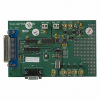
Manufacturer Part Number
EVAL-AD7706EB
Description
BOARD EVAL FOR AD7706
Manufacturer
Analog Devices Inc
Datasheet
1.EVAL-AD7705EB.pdf
(32 pages)
Specifications of EVAL-AD7706EB
Number Of Adc's
1
Number Of Bits
16
Sampling Rate (per Second)
500
Data Interface
Serial
Inputs Per Adc
3 Differential
Input Range
0 ~ 5.25 V
Power (typ) @ Conditions
6.5mW @ 500SPS
Voltage Supply Source
Single
Operating Temperature
-40°C ~ 85°C
Utilized Ic / Part
AD7706
Lead Free Status / RoHS Status
Contains lead / RoHS non-compliant


AD7705/AD7706
MICROCOMPUTER/MICROPROCESSOR INTERFACING
The AD7705/AD7706’s flexible serial interface allows for easy
interface to most microcomputers and microprocessors. The
flowchart of Figure 10 outlines the sequence that should be
followed when interfacing a microcontroller or microprocessor
to the AD7705/AD7706. Figures 19, 20 and 21 show some
typical interface circuits.
The serial interface on the AD7705/AD7706 is capable of oper-
ating from just three wires and is compatible with SPI interface
protocols. The three-wire operation makes the part ideal for
isolated systems where minimizing the number of interface lines
minimizes the number of opto-isolators required in the system.
The serial clock input is a Schmitt triggered input to accommo-
date slow edges from opto-couplers. The rise and fall times of
other digital inputs to the AD7705/AD7706 should be no longer
than 1 s.
Most of the registers on the AD7705/AD7706 are 8-bit regis-
ters, which facilitates easy interfacing to the 8-bit serial ports of
microcontrollers. The Data Register on the AD7705/AD7706 is
16 bits, and the offset and gain registers are 24-bit registers but
data transfers to these registers can consist of multiple 8-bit
transfers to the serial port of the microcontroller. DSP proces-
sors and microprocessors generally transfer 16 bits of data in a
serial data operation. Some of these processors, such as the
ADSP-2105, have the facility to program the amount of cycles
in a serial transfer. This allows the user to tailor the number of
bits in any transfer to match the register length of the required
register in the AD7705/AD7706.
Even though some of the registers on the AD7705/AD7706 are
only eight bits in length, communicating with two of these regis-
ters in successive write operations can be handled as a single 16-
bit data transfer if required. For example, if the Setup Register
is to be updated, the processor must first write to the Communi-
cations Register (saying that the next operation is a write to the
Setup Register) and then write eight bits to the Setup Register.
If required, this can all be done in a single 16-bit transfer be-
cause once the eight serial clocks of the write operation to the
Communications Register have been completed, the part imme-
diately sets itself up for a write operation to the Setup Register.
AD7705/AD7706 to 68HC11 Interface
Figure 19 shows an interface between the AD7705/AD7706 and
the 68HC11 microcontroller. The diagram shows the minimum
(three-wire) interface with CS on the AD7705/AD7706 hard-
wired low. In this scheme, the DRDY bit of the Communica-
tions Register is monitored to determine when the Data Register
is updated. An alternative scheme, which increases the number
of interface lines to four, is to monitor the DRDY output line
from the AD7705/AD7706. The monitoring of the DRDY line
can be done in two ways. First, DRDY can be connected to one
of the 68HC11’s port bits (such as PC0), which is configured as
an input. This port bit is then polled to determine the status of
DRDY. The second scheme is to use an interrupt driven system,
in which case the DRDY output is connected to the IRQ input
of the 68HC11. For interfaces that require control of the CS
input on the AD7705/AD7706, one of the port bits of the
68HC11 (such as PC1), which is configured as an output, can
be used to drive the CS input.
–26–
The 68HC11 is configured in the master mode with its CPOL
bit set to a logic one and its CPHA bit set to a logic one. When
the 68HC11 is configured like this, its SCLK line idles high
between data transfers. The AD7705/AD7706 is not capable of
full duplex operation. If the AD7705/AD7706 is configured for
a write operation, no data appears on the DATA OUT lines
even when the SCLK input is active. Similarly, if the AD7705/
AD7706 is configured for a read operation, data presented to
the part on the DATA IN line is ignored even when SCLK is
active.
Coding for an interface between the 68HC11 and the AD7705/
AD7706 is given in Table XV. In this example, the DRDY
output line of the AD7705/AD7706 is connected to the PC0 port
bit of the 68HC11 and is polled to determine its status.
AD7705/AD7706 to 8051 Interface
An interface circuit between the AD7705/AD7706 and the
8XC51 microcontroller is shown in Figure 20. The diagram
shows the minimum number of interface connections with CS
on the AD7705/AD7706 hard-wired low. In the case of the
8XC51 interface the minimum number of interconnects is just
two. In this scheme, the DRDY bit of the Communications
Register is monitored to determine when the Data Register is
updated. The alternative scheme, which increases the number of
Figure 19. AD7705/AD7706 to 68HC11 Interface
Figure 20. AD7705/AD7706 to 8XC51 Interface
68HC11
8XC51
MISO
MOSI
SCK
P3.0
P3.1
SS
V
DD
V
DD
V
V
DD
DD
RESET
RESET
SCLK
DATA OUT
DATA IN
CS
DATA OUT
DATA IN
SCLK
CS
AD7705/AD7706
AD7705/AD7706
REV. A
Related parts for EVAL-AD7706EB
Image
Part Number
Description
Manufacturer
Datasheet
Request
R

Part Number:
Description:
ENERCHIP CC EVAL KIT
Manufacturer:
Cymbet Corporation
Datasheet:

Part Number:
Description:
BOARD EVAL FOR AD976
Manufacturer:
Analog Devices Inc
Datasheet:

Part Number:
Description:
BOARD EVAL FOR ADXL345
Manufacturer:
Analog Devices Inc
Datasheet:

Part Number:
Description:
ENERCHIP CC SEH EVAL KIT
Manufacturer:
Cymbet Corporation
Datasheet:

Part Number:
Description:
ENERCHIP EP ENERGY HARVEST EVAL
Manufacturer:
Cymbet Corporation
Datasheet:

Part Number:
Description:
EVAL BOARD FOR TW6864-LB2-GR
Manufacturer:
Intersil
Datasheet:
Part Number:
Description:
EVAL BOARD FOR TW8816-LB3-GR
Manufacturer:
Intersil
Datasheet:
Part Number:
Description:
EVAL BOARD FOR TW8817-TA3-GRS
Manufacturer:
Intersil
Datasheet:

Part Number:
Description:
EVALUATION MODULE FOR ADUM4160
Manufacturer:
Analog Devices Inc
Datasheet:

Part Number:
Description:
BOARD EVALUATION ADCMP581BCP
Manufacturer:
Analog Devices Inc
Datasheet:
Part Number:
Description:
BOARD EVALUATION ADM1041
Manufacturer:
Analog Devices Inc
Datasheet:

Part Number:
Description:
EVAL BOARD FOR STM32F107VCT
Manufacturer:
STMicroelectronics
Datasheet:
Part Number:
Description:
BOARD EVAL FOR AD1954
Manufacturer:
Analog Devices Inc
Datasheet:
Part Number:
Description:
BOARD EVAL FOR AD1955
Manufacturer:
Analog Devices Inc
Datasheet:

Part Number:
Description:
BOARD EVAL FOR AD7655
Manufacturer:
Analog Devices Inc
Datasheet: