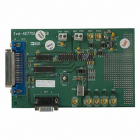
EVAL-AD7706EB Analog Devices Inc, EVAL-AD7706EB Datasheet - Page 11
EVAL-AD7706EB
Manufacturer Part Number
EVAL-AD7706EB
Description
BOARD EVAL FOR AD7706
Manufacturer
Analog Devices Inc
Datasheet
1.EVAL-AD7705EB.pdf
(32 pages)
Specifications of EVAL-AD7706EB
Number Of Adc's
1
Number Of Bits
16
Sampling Rate (per Second)
500
Data Interface
Serial
Inputs Per Adc
3 Differential
Input Range
0 ~ 5.25 V
Power (typ) @ Conditions
6.5mW @ 500SPS
Voltage Supply Source
Single
Operating Temperature
-40°C ~ 85°C
Utilized Ic / Part
AD7706
Lead Free Status / RoHS Status
Contains lead / RoHS non-compliant


REV. A
R/W
STBY
CH1–CH0
Standby. Writing a “1” to this bit puts the part into its standby or power-down mode. In this mode, the part con-
Channel Select. These two bits select a channel for conversion or for access to the calibration coefficients as out-
RS2
0
0
0
0
1
1
1
1
Read/Write Select. This bit selects whether the next operation is a read or write operation to the selected register.
A “0” indicates a write cycle for the next operation to the appropriate register, while a “1” indicates a read opera-
tion from the appropriate register.
sumes only 10 A of power supply current. The part retains its calibration coefficients and control word informa-
tion when in STANDBY. Writing a “0” to this bit places the part in its normal operating mode.
lined in Table VII. Three pairs of calibration registers on the part are used to store the calibration coefficients
following a calibration on a channel. They are shown in Tables VII for the AD7705 and Table VIII for the AD7706
to indicate which channel combinations have independent calibration coefficients. With CH1 at Logic 1 and CH0
at a Logic 0, the part looks at the AIN1(–) input internally shorted to itself on the AD7705 or at COMMON
internally shorted to itself on the AD7706. This can be used as a test method to evaluate the noise performance of
the part with no external noise sources. In this mode, the AIN1(–)/COMMON input should be connected to
an external voltage within the allowable common-mode range for the part.
CH1
0
0
1
1
CH1
0
0
1
1
RS1
0
0
1
1
0
0
1
1
CH0
0
1
0
1
CH0
0
1
0
1
Table VII. Channel Selection for AD7705
Table VIII. Channel Selection for AD7706
RS0
0
1
0
1
0
1
0
1
AIN(+)
AIN1(+)
AIN2(+)
AIN1(–)
AIN1(–)
AIN
AIN1
AIN2
COMMON
AIN3
Table VI. Register Selection
Register
Communications Register
Setup Register
Clock Register
Data Register
Test Register
No Operation
Offset Register
Gain Register
–11–
AIN(–)
AIN1(–)
AIN2(–)
AIN1(–)
AIN2(–)
Reference
COMMON
COMMON
COMMON
COMMON
Calibration Register Pair
Register Pair 0
Register Pair 1
Register Pair 0
Register Pair 2
Calibration Register Pair
Register Pair 0
Register Pair 1
Register Pair 0
Register Pair 2
Register Size
8 Bits
8 Bits
8 Bits
16 Bits
8 Bits
24 Bits
24 Bits
AD7705/AD7706
Related parts for EVAL-AD7706EB
Image
Part Number
Description
Manufacturer
Datasheet
Request
R

Part Number:
Description:
ENERCHIP CC EVAL KIT
Manufacturer:
Cymbet Corporation
Datasheet:

Part Number:
Description:
BOARD EVAL FOR AD976
Manufacturer:
Analog Devices Inc
Datasheet:

Part Number:
Description:
BOARD EVAL FOR ADXL345
Manufacturer:
Analog Devices Inc
Datasheet:

Part Number:
Description:
ENERCHIP CC SEH EVAL KIT
Manufacturer:
Cymbet Corporation
Datasheet:

Part Number:
Description:
ENERCHIP EP ENERGY HARVEST EVAL
Manufacturer:
Cymbet Corporation
Datasheet:

Part Number:
Description:
EVAL BOARD FOR TW6864-LB2-GR
Manufacturer:
Intersil
Datasheet:
Part Number:
Description:
EVAL BOARD FOR TW8816-LB3-GR
Manufacturer:
Intersil
Datasheet:
Part Number:
Description:
EVAL BOARD FOR TW8817-TA3-GRS
Manufacturer:
Intersil
Datasheet:

Part Number:
Description:
EVALUATION MODULE FOR ADUM4160
Manufacturer:
Analog Devices Inc
Datasheet:

Part Number:
Description:
BOARD EVALUATION ADCMP581BCP
Manufacturer:
Analog Devices Inc
Datasheet:
Part Number:
Description:
BOARD EVALUATION ADM1041
Manufacturer:
Analog Devices Inc
Datasheet:

Part Number:
Description:
EVAL BOARD FOR STM32F107VCT
Manufacturer:
STMicroelectronics
Datasheet:
Part Number:
Description:
BOARD EVAL FOR AD1954
Manufacturer:
Analog Devices Inc
Datasheet:
Part Number:
Description:
BOARD EVAL FOR AD1955
Manufacturer:
Analog Devices Inc
Datasheet:

Part Number:
Description:
BOARD EVAL FOR AD7655
Manufacturer:
Analog Devices Inc
Datasheet: