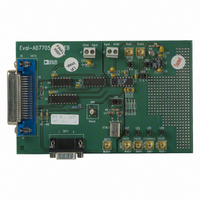
EVAL-AD7706EB Analog Devices Inc, EVAL-AD7706EB Datasheet - Page 22
EVAL-AD7706EB
Manufacturer Part Number
EVAL-AD7706EB
Description
BOARD EVAL FOR AD7706
Manufacturer
Analog Devices Inc
Datasheet
1.EVAL-AD7705EB.pdf
(32 pages)
Specifications of EVAL-AD7706EB
Number Of Adc's
1
Number Of Bits
16
Sampling Rate (per Second)
500
Data Interface
Serial
Inputs Per Adc
3 Differential
Input Range
0 ~ 5.25 V
Power (typ) @ Conditions
6.5mW @ 500SPS
Voltage Supply Source
Single
Operating Temperature
-40°C ~ 85°C
Utilized Ic / Part
AD7706
Lead Free Status / RoHS Status
Contains lead / RoHS non-compliant


AD7705/AD7706
Placing the part in standby mode reduces the total current to
9 A typical with V
part is operated from an external master clock provided this
master clock is stopped. If the external clock continues to run in
standby mode, the standby current increases to 150 A typical
with 5 V supplies and 75 A typical with 3.3 V supplies. If a
crystal or ceramic resonator is used as the clock source, the total
current in standby mode is 400 A typical with 5 V supplies and
90 A with 3.3 V supplies. This is because the on-chip oscillator
circuit continues to run when the part is in its standby mode.
This is important in applications where the system clock is pro-
vided by the AD7705/AD7706’s clock, so that the AD7705/
AD7706 produces an uninterrupted master clock even when it is
in its standby mode.
Accuracy
Sigma-Delta ADCs, like VFCs and other integrating ADCs, do
not contain any source of nonmonotonicity and inherently offer
no missing codes performance. The AD7705/AD7706 achieves
excellent linearity by the use of high quality, on-chip capacitors,
which have a very low capacitance/voltage coefficient. The de-
vice also achieves low input drift through the use of chopper-
stabilized techniques in its input stage. To ensure excellent
performance over time and temperature, the AD7705/AD7706
uses digital calibration techniques that minimize offset and gain
error.
Drift Considerations
The AD7705/AD7706 uses chopper stabilization techniques to
minimize input offset drift. Charge injection in the analog
switches and dc leakage currents at the sampling node are the
primary sources of offset voltage drift in the converter. The dc
input leakage current is essentially independent of the selected
gain. Gain drift within the converter depends primarily upon
the temperature tracking of the internal capacitors. It is not
affected by leakage currents.
Measurement errors due to offset drift or gain drift can be
eliminated at any time by recalibrating the converter. Using
the system calibration mode can also minimize offset and gain
errors in the signal conditioning circuitry. Integral and differen-
tial linearity errors are not significantly affected by temperature
changes.
POWER SUPPLIES
The AD7705/AD7706 operates with a V
tween 2.7 V and 5.25 V. While the latch-up performance of the
AD7705/AD7706 is good, it is important that power is applied
to the AD7705/AD7706 before signals at REF IN, AIN or the
logic input pins in order to avoid excessive currents. If this is not
possible, the current that flows in any of these pins should be
limited. If separate supplies are used for the AD7705/AD7706
and the system digital circuitry, the AD7705/AD7706 should be
powered up first. If it is not possible to guarantee this, current
limiting resistors should be placed in series with the logic
inputs to again limit the current. Latch-up current is greater
than 100 mA.
DD
= 5 V and 4 A with V
DD
power supply be-
DD
= 3 V when the
–22–
Supply Current
The current consumption on the AD7705/AD7706 is specified
for supplies in the range +2.7 V to +3.3 V and in the range +4.75 V
to +5.25 V. The part operates over a +2.7 V to +5.25 V supply
range and the I
over this range. There is an internal current boost bit on the
AD7705/AD7706 that is set internally in accordance with the
operating conditions. This affects the current drawn by the
analog circuitry within these devices. Minimum power consump-
tion is achieved when the AD7705/AD7706 is operated with an
f
as the internal boost bit is off reducing the analog current con-
sumption. Figure 15 shows the variation of the typical I
V
crystal oscillator at +25 C. The AD7705/AD7706 is operated in
unbuffered mode. The relationship shows that the I
mized by operating the part with lower V
AD7705/AD7706 is also minimized by using an external master
clock or by optimizing external components when using the
on-chip oscillator circuit. Figures 3, 4, 6 and 7 show variations
in I
clock.
Grounding and Layout
Since the analog inputs and reference input are differential, most
of the voltages in the analog modulator are common-mode volt-
ages. The excellent common-mode rejection of the part will
remove common-mode noise on these inputs. The digital filter
will provide rejection of broadband noise on the power supplies,
except at integer multiples of the modulator sampling frequency.
The digital filter also removes noise from the analog and refer-
ence inputs provided those noise sources do not saturate the
analog modulator. As a result, the AD7705/AD7706 is more
immune to noise interference than a conventional high resolu-
tion converter. However, because the resolution of the AD7705/
AD7706 is so high, and the noise levels from the AD7705/
AD7706 so low, care must be taken with regard to grounding
and layout.
CLKIN
DD
DD
voltage for both a 1 MHz crystal oscillator and a 2.4576 MHz
of 1 MHz or at gains of 1 to 4 with f
with gain, V
1600
1400
1200
1000
800
600
400
200
0
2.5
MCLK IN = CRYSTAL OSCILLATOR
T
UNBUFFERED MODE
GAIN = 128
Figure 15. I
DD
A
= +25 C
3.0
for the part varies as the supply voltage varies
DD
and clock frequency using an external
3.5
DD
vs. Supply Voltage
f
CLK
V
4.0
DD
= 2.4576MHz
DD
4.5
f
CLK
CLKIN
voltages. I
= 1MHz
= 2.4575 MHz
5.0
DD
DD
is mini-
DD
REV. A
5.5
on the
with
Related parts for EVAL-AD7706EB
Image
Part Number
Description
Manufacturer
Datasheet
Request
R

Part Number:
Description:
ENERCHIP CC EVAL KIT
Manufacturer:
Cymbet Corporation
Datasheet:

Part Number:
Description:
BOARD EVAL FOR AD976
Manufacturer:
Analog Devices Inc
Datasheet:

Part Number:
Description:
BOARD EVAL FOR ADXL345
Manufacturer:
Analog Devices Inc
Datasheet:

Part Number:
Description:
ENERCHIP CC SEH EVAL KIT
Manufacturer:
Cymbet Corporation
Datasheet:

Part Number:
Description:
ENERCHIP EP ENERGY HARVEST EVAL
Manufacturer:
Cymbet Corporation
Datasheet:

Part Number:
Description:
EVAL BOARD FOR TW6864-LB2-GR
Manufacturer:
Intersil
Datasheet:
Part Number:
Description:
EVAL BOARD FOR TW8816-LB3-GR
Manufacturer:
Intersil
Datasheet:
Part Number:
Description:
EVAL BOARD FOR TW8817-TA3-GRS
Manufacturer:
Intersil
Datasheet:

Part Number:
Description:
EVALUATION MODULE FOR ADUM4160
Manufacturer:
Analog Devices Inc
Datasheet:

Part Number:
Description:
BOARD EVALUATION ADCMP581BCP
Manufacturer:
Analog Devices Inc
Datasheet:
Part Number:
Description:
BOARD EVALUATION ADM1041
Manufacturer:
Analog Devices Inc
Datasheet:

Part Number:
Description:
EVAL BOARD FOR STM32F107VCT
Manufacturer:
STMicroelectronics
Datasheet:
Part Number:
Description:
BOARD EVAL FOR AD1954
Manufacturer:
Analog Devices Inc
Datasheet:
Part Number:
Description:
BOARD EVAL FOR AD1955
Manufacturer:
Analog Devices Inc
Datasheet:

Part Number:
Description:
BOARD EVAL FOR AD7655
Manufacturer:
Analog Devices Inc
Datasheet: