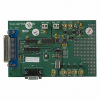
EVAL-AD7706EB Analog Devices Inc, EVAL-AD7706EB Datasheet - Page 13
EVAL-AD7706EB
Manufacturer Part Number
EVAL-AD7706EB
Description
BOARD EVAL FOR AD7706
Manufacturer
Analog Devices Inc
Datasheet
1.EVAL-AD7705EB.pdf
(32 pages)
Specifications of EVAL-AD7706EB
Number Of Adc's
1
Number Of Bits
16
Sampling Rate (per Second)
500
Data Interface
Serial
Inputs Per Adc
3 Differential
Input Range
0 ~ 5.25 V
Power (typ) @ Conditions
6.5mW @ 500SPS
Voltage Supply Source
Single
Operating Temperature
-40°C ~ 85°C
Utilized Ic / Part
AD7706
Lead Free Status / RoHS Status
Contains lead / RoHS non-compliant


REV. A
Clock Register (RS2, RS1, RS0 = 0, 1, 0); Power-On/Reset Status: 05 Hex
The Clock Register is an 8-bit register from which data can either be read or to which data can be written. Table XI outlines the bit
designations for the Clock Register.
ZERO
CLKDIS
CLKDIV
CLK
FS1, FS0
ZERO (0)
CLK*
*Assumes correct clock frequency on MCLK IN pin with CLKDIV bit set appropriately.
0
0
0
0
1
1
1
1
Zero. A zero MUST be written to these bits to ensure correct operation of the AD7705/AD7706. Failure to do so
may result in unspecified operation of the device.
Master Clock Disable Bit. A Logic 1 in this bit disables the master clock from appearing at the MCLK OUT pin.
When disabled, the MCLK OUT pin is forced low. This feature allows the user the flexibility of using the MCLK
OUT as a clock source for other devices in the system or of turning off the MCLK OUT as a power saving feature.
When using an external master clock on the MCLK IN pin, the AD7705/AD7706 continues to have internal
clocks and will convert normally with the CLKDIS bit active. When using a crystal oscillator or ceramic resonator
across the MCLK IN and MCLK OUT pins, the AD7705/AD7706 clock is stopped and no conversions take place
when the CLKDIS bit is active.
Clock Divider Bit. With this bit at a Logic 1, the clock frequency appearing at the MCLK IN pin is divided by two
before being used internally by the AD7705/AD7706. For example, when this bit is set to 1, the user can operate
with a 4.9152 MHz crystal between MCLK IN and MCLK OUT and internally the part will operate with the
specified 2.4576 MHz. With this bit at a Logic 0, the clock frequency appearing at the MCLK IN pin is the fre-
quency used internally by the part.
Clock Bit. This bit should be set in accordance with the operating frequency of the AD7705/AD7706. If the device
has a master clock frequency of 2.4576 MHz (CLKDIV = 0) or 4.9152 MHz (CLKDIV = 1), then this bit should
be set to a “1.” If the device has a master clock frequency of 1 MHz (CLKDIV = 0) or 2 MHz (CLKDIV = 1),
this bit should be set to a “0.” This bit sets up the appropriate scaling currents for a given operating frequency and
also chooses (along with FS1 and FS0) the output update rate for the device. If this bit is not set correctly for the
master clock frequency of the device, then the AD7705/AD7706 may not operate to specification.
Filter Selection Bits. Along with the CLK bit, FS1 and FS0 determine the output update rate, filter first notch and
–3 dB frequency as outlined in Table XII. The on-chip digital filter provides a sinc
association with the gain selection, it also determines the output noise of the device. Changing the filter notch
frequency, as well as the selected gain, impacts resolution. Tables I to IV show the effect of filter notch frequency
and gain on the output noise and effective resolution of the part. The output data rate (or effective conversion
time) for the device is equal to the frequency selected for the first notch of the filter. For example, if the first notch
of the filter is selected at 50 Hz, a new word is available at a 50 Hz output rate or every 20 ms. If the first notch is
at 500 Hz, a new word is available every 2 ms. A calibration should be initiated when any of these bits are changed.
The settling time of the filter to a full-scale step input is worst case 4 1/(output data rate). For example, with the
filter first notch at 50 Hz, the settling time of the filter to a full-scale step input is 80 ms max. If the first notch is at
500 Hz, the settling time is 8 ms max. This settling time can be reduced to 3 1/(output data rate) by synchroniz-
ing the step input change to a reset of the digital filter. In other words, if the step input takes place with the FSYNC bit
high, the settling-time will be 3 1/(output data rate) from when the FSYNC bit returns low.
The –3 dB frequency is determined by the programmed first notch frequency according to the relationship:
ZERO (0)
FS1
0
0
1
1
0
0
1
1
ZERO (0)
filter –3 dB frequency = 0.262 filter first notch frequency
FS0
0
1
0
1
0
1
0
1
Table XII. Output Update Rates
CLKDIS (0)
Table XI. Clock Register
–13–
Output Update Rate
20 Hz
25 Hz
100 Hz
200 Hz
50 Hz
60 Hz
250 Hz
500 Hz
CLKDIV (0)
CLK (1)
–3 dB Filter Cutoff
5.24 Hz
6.55 Hz
26.2 Hz
52.4 Hz
13.1 Hz
15.7 Hz
65.5 Hz
131 Hz
3
AD7705/AD7706
(or Sinx/x
FS1 (0)
3
) filter response. In
FS0 (1)
Related parts for EVAL-AD7706EB
Image
Part Number
Description
Manufacturer
Datasheet
Request
R

Part Number:
Description:
ENERCHIP CC EVAL KIT
Manufacturer:
Cymbet Corporation
Datasheet:

Part Number:
Description:
BOARD EVAL FOR AD976
Manufacturer:
Analog Devices Inc
Datasheet:

Part Number:
Description:
BOARD EVAL FOR ADXL345
Manufacturer:
Analog Devices Inc
Datasheet:

Part Number:
Description:
ENERCHIP CC SEH EVAL KIT
Manufacturer:
Cymbet Corporation
Datasheet:

Part Number:
Description:
ENERCHIP EP ENERGY HARVEST EVAL
Manufacturer:
Cymbet Corporation
Datasheet:

Part Number:
Description:
EVAL BOARD FOR TW6864-LB2-GR
Manufacturer:
Intersil
Datasheet:
Part Number:
Description:
EVAL BOARD FOR TW8816-LB3-GR
Manufacturer:
Intersil
Datasheet:
Part Number:
Description:
EVAL BOARD FOR TW8817-TA3-GRS
Manufacturer:
Intersil
Datasheet:

Part Number:
Description:
EVALUATION MODULE FOR ADUM4160
Manufacturer:
Analog Devices Inc
Datasheet:

Part Number:
Description:
BOARD EVALUATION ADCMP581BCP
Manufacturer:
Analog Devices Inc
Datasheet:
Part Number:
Description:
BOARD EVALUATION ADM1041
Manufacturer:
Analog Devices Inc
Datasheet:

Part Number:
Description:
EVAL BOARD FOR STM32F107VCT
Manufacturer:
STMicroelectronics
Datasheet:
Part Number:
Description:
BOARD EVAL FOR AD1954
Manufacturer:
Analog Devices Inc
Datasheet:
Part Number:
Description:
BOARD EVAL FOR AD1955
Manufacturer:
Analog Devices Inc
Datasheet:

Part Number:
Description:
BOARD EVAL FOR AD7655
Manufacturer:
Analog Devices Inc
Datasheet: