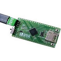
EVAL-ADXL345Z-DB Analog Devices Inc, EVAL-ADXL345Z-DB Datasheet
EVAL-ADXL345Z-DB
Specifications of EVAL-ADXL345Z-DB


Related parts for EVAL-ADXL345Z-DB


EVAL-ADXL345Z-DB Summary of contents
Page 1
FEATURES Ultralow power: as low as 23 μA in measurement mode and 0.1 μA in standby mode 2.5 V (typical) S Power consumption scales automatically with bandwidth User-selectable resolution Fixed 10-bit resolution Full resolution, where resolution increases ...
Page 2
ADXL345 TABLE OF CONTENTS Features .............................................................................................. 1 Applications....................................................................................... 1 General Description ......................................................................... 1 Functional Block Diagram .............................................................. 1 Revision History ............................................................................... 3 Specifications..................................................................................... 4 Absolute Maximum Ratings............................................................ 6 Thermal Resistance ...................................................................... 6 Package Information .................................................................... 6 ESD Caution.................................................................................. 6 Pin ...
Page 3
REVISION HISTORY 11/10—Rev Rev. B Change Offset vs. Temperature for Z-Axis Parameter, Table 1 .................................................................................................4 Changes to Figure 10 to Figure 15 ..................................................9 Changes to Ordering Guide...........................................................37 4/10—Rev Rev. A Changes to Features ...
Page 4
ADXL345 SPECIFICATIONS T = 25° 2 1.8 V, acceleration = I/O otherwise noted. All minimum and maximum specifications are guaranteed. Typical specifications are not guaranteed. Table 1. Parameter SENSOR ...
Page 5
Parameter TEMPERATURE Operating Temperature Range WEIGHT Device Weight 1 The typical specifications shown are for at least 68% of the population of parts and are based on the worst case of mean ±1 σ, except for 0 g output and ...
Page 6
ADXL345 ABSOLUTE MAXIMUM RATINGS Table 2. Parameter Rating Acceleration Any Axis, Unpowered 10,000 g Any Axis, Powered 10,000 g V −0 +3 −0 +3 I/O Digital Pins −0 ...
Page 7
PIN CONFIGURATION AND FUNCTION DESCRIPTIONS Table 5. Pin Function Descriptions Pin No. Mnemonic I/O 2 GND 3 RESERVED 4 GND 5 GND INT1 9 INT2 RESERVED 12 SDO/ALT ...
Page 8
ADXL345 TYPICAL PERFORMANCE CHARACTERISTICS –150 –100 –50 0 ZERO g OFFSET (mg) Figure 4. X-Axis Zero g Offset at 25° ...
Page 9
ZERO g OFFSET TEMPERATURE COEFFICIENT (mg/°C) Figure 10. X-Axis Zero g Offset Temperature Coefficient –2.0 –1.5 –1.0 –0.5 ...
Page 10
ADXL345 230 234 238 242 246 250 254 258 262 266 270 274 278 282 SENSITIVITY (LSB/g) Figure 16. X-Axis Sensitivity at 25° 2.5 V, Full ...
Page 11
TEMPERATURE (°C) Figure 22. X-Axis Sensitivity vs. Temperature— Eight Parts Soldered to PCB 2.5 V, Full Resolution S 280 275 ...
Page 12
ADXL345 0.2 0.5 0.8 1.1 SELF-TEST RESPONSE (g) Figure 28. X-Axis Self-Test Response at 25° –0.2 –0.5 –0.8 –1.1 –1.4 SELF-TEST RESPONSE ( g ) ...
Page 13
THEORY OF OPERATION The ADXL345 is a complete 3-axis acceleration measurement system with a selectable measurement range of ±2 g, ±4 g, ± ± measures both dynamic acceleration resulting from motion or shock and static acceleration, ...
Page 14
ADXL345 POWER SAVINGS Power Modes The ADXL345 automatically modulates its power consumption in proportion to its output data rate, as outlined in Table 7. If additional power savings is desired, a lower power mode is available. In this mode, the ...
Page 15
SERIAL COMMUNICATIONS and SPI digital communications are available. In both cases mode is enabled if the CS the ADXL345 operates as a slave The CS pin should always be tied high pin is ...
Page 16
ADXL345 CS t DELAY SCLK t t SETUP W SDI t SDO DELAY SCLK t t SETUP R SDI t SDO X SDO CS t DELAY SCLK t t SETUP HOLD R/W SDIO SDO NOTES t 1. ...
Page 17
Table 9. SPI Digital Input/Output Parameter Digital Input Low Level Input Voltage ( High Level Input Voltage ( Low Level Input Current ( High Level Input Current ( Digital Output Low Level ...
Page 18
ADXL345 With CS tied high the ADXL345 I/O requiring a simple 2-wire connection, as shown in The ADXL345 conforms to the UM10204 I and User Manual, Rev. 03—19 June 2007, ...
Page 19
Table 12 Timing (T = 25° 2 Limit Parameter Min f SCL 100 ...
Page 20
ADXL345 INTERRUPTS The ADXL345 provides two output pins for driving interrupts: INT1 and INT2. Both interrupt pins are push-pull, low impedance pins with output specifications shown in Table 13. The default configuration of the interrupt pins is active high. This ...
Page 21
Overrun The overrun bit is set when new data replaces unread data. The precise operation of the overrun function depends on the FIFO mode. In bypass mode, the overrun bit is set when new data replaces unread data in the ...
Page 22
ADXL345 SELF-TEST The ADXL345 incorporates a self-test feature that effectively tests its mechanical and electronic systems simultaneously. When the self-test function is enabled (via the SELF_TEST bit in the DATA_FORMAT register, Address 0x31), an electrostatic force is exerted on the ...
Page 23
REGISTER MAP Table 19. Address Hex Dec Name 0x00 0 DEVID 0x01 to 0x1C Reserved 0x1D 29 THRESH_TAP 0x1E 30 OFSX 0x1F 31 OFSY 0x20 32 OFSZ 0x21 33 DUR 0x22 34 Latent 0x23 35 Window 0x24 ...
Page 24
ADXL345 REGISTER DEFINITIONS Register 0x00—DEVID (Read Only The DEVID register holds a fixed device ID code of 0xE5 (345 octal). Register 0x1D—THRESH_TAP (Read/Write) The THRESH_TAP register is eight bits and ...
Page 25
ACT_x Enable Bits and INACT_x Enable Bits A setting of 1 enables x-, y-, or z-axis participation in detecting activity or inactivity. A setting of 0 excludes the selected axis from participation. If all axes are excluded, the function is ...
Page 26
ADXL345 If the link bit is not set, the AUTO_SLEEP feature is disabled and setting the AUTO_SLEEP bit does not have an impact on device operation. Refer to the Link Bit section or the Link Mode section for more information ...
Page 27
INT_INVERT Bit A value the INT_INVERT bit sets the interrupts to active high, and a value of 1 sets the interrupts to active low. FULL_RES Bit When this bit is set to a value of 1, the ...
Page 28
ADXL345 APPLICATIONS INFORMATION POWER SUPPLY DECOUPLING A 1 μF tantalum capacitor ( and a 0.1 μF ceramic capacitor placed close to the ADXL345 supply pins is I/O DD I/O recommended to ...
Page 29
Several events can occur to invalidate the second tap of a double tap event. First, if the suppress bit in the TAP_AXES register (Address 0x2A) is set, any acceleration spike above the threshold during the latency time (set by the ...
Page 30
ADXL345 SLEEP MODE VS. LOW POWER MODE In applications where a low data rate and low power consumption is desired (at the expense of noise performance recommended that low power mode be used. The use of low power ...
Page 31
USING SELF-TEST The self-test change is defined as the difference between the acceleration output of an axis with self-test enabled and the acceleration output of the same axis with self-test disabled (see Endnote 4 of Table 1). This definition assumes ...
Page 32
ADXL345 DATA FORMATTING OF UPPER DATA RATES Formatting of output data at the 3200 Hz and 1600 Hz output data rates changes depending on the mode of operation (full- resolution or fixed 10-bit) and the selected output range. When using ...
Page 33
NOISE PERFORMANCE The specification of noise shown in Table 1 corresponds to the typical noise performance of the ADXL345 in normal power operation with an output data rate of 100 Hz (LOW_POWER bit (D4 rate bits (D3:D0) = ...
Page 34
ADXL345 Changes in noise performance, self-test response, and supply current are discussed elsewhere throughout the data sheet. For noise performance, the Noise Performance section should be reviewed. The Using Self-Test section discusses both the operation of self-test over voltage, a ...
Page 35
AXES OF ACCELERATION SENSITIVITY Figure 56. Axes of Acceleration Sensitivity (Corresponding Output Voltage Increases When Accelerated Along the Sensitive Axis OUT Y = –1g OUT OUT OUT ...
Page 36
ADXL345 LAYOUT AND DESIGN RECOMMENDATIONS Figure 58 shows the recommended printed wiring board land pattern. Figure 59 and Table 24 provide details about the recommended soldering profile. Figure 58. Recommended Printed Wiring Board Land Pattern (Dimensions shown in millimeters) T ...
Page 37
... SEATING PLANE ORDERING GUIDE Measurement Model 1 Range (g) ADXL345BCCZ ±2, ±4, ±8, ±16 ADXL345BCCZ-RL ±2, ±4, ±8, ±16 ADXL345BCCZ-RL7 ±2, ±4, ±8, ±16 EVAL-ADXL345Z EVAL-ADXL345Z-DB EVAL-ADXL345Z-M EVAL-ADXL345Z RoHS Compliant Part. 3.00 BSC 0.49 BOTTOM VIEW 13 0.80 5.00 BSC BSC 0.50 8 TOP VIEW 0 ...
Page 38
ADXL345 NOTES Rev Page ...
Page 39
NOTES Rev Page ADXL345 ...
Page 40
ADXL345 NOTES Analog Devices offers specific products designated for automotive applications; please consult your local Analog Devices sales representative for details. Standard products sold by Analog Devices are not designed, intended, or approved for use in life support, implantable medical ...