TOOLSTICK560DC Silicon Laboratories Inc, TOOLSTICK560DC Datasheet - Page 65
TOOLSTICK560DC
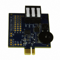
Manufacturer Part Number
TOOLSTICK560DC
Description
DAUGHTER CARD TOOLSTICK F560
Manufacturer
Silicon Laboratories Inc
Series
ToolStickr
Type
MCUr
Specifications of TOOLSTICK560DC
Contents
Daughter Card
Processor To Be Evaluated
C8051F55x, C8051F56x, C8051F57x
Interface Type
USB
Operating Supply Voltage
2.7 V to 3.6 V
Lead Free Status / RoHS Status
Lead free / RoHS Compliant
For Use With/related Products
C8051F55x, C8051F56x, C8051F57x
For Use With
336-1345 - TOOLSTICK BASE ADAPTER336-1182 - ADAPTER USB DEBUG FOR C8051FXXX
Lead Free Status / Rohs Status
Lead free / RoHS Compliant
Other names
336-1719


6.5. ADC0 Analog Multiplexer
ADC0 includes an analog multiplexer to enable multiple analog input sources. Any of the following may be
selected as an input: P0.0 – P3.7, the on-chip temperature sensor, the core power supply (V
(GND). ADC0 is single-ended and all signals measured are with respect to GND. The ADC0 input
channels are selected using the ADC0MX register as described in SFR Definition 6.13.
Important Note About ADC0 Input Configuration: Port pins selected as ADC0 inputs should be config-
ured as analog inputs, and should be skipped by the Digital Crossbar. To configure a Port pin for analog
input, set to 0 the corresponding bit in register PnMDIN. To force the Crossbar to skip a Port pin, set to 1
the corresponding bit in register PnSKIP. See Section “19. Port Input/Output” on page 167 for more Port
I/O configuration details.
Sensor
Temp
Figure 6.8. ADC0 Multiplexer Block Diagram
P0.0
P0.7
P1.0
P1.7
P2.0
P2.7
P3.0
P3.7
GND
VDD
AMUX
Rev. 1.1
P3.1-P3.7 available as inputs on
P2.2-P2.7, P3.0 available as
48-pin and 40-pin packages
inputs on 40-pin and 32-pin
C8051F55x/56x/57x
ADC0MX
ADC0
packages
DD
), or ground
65
Related parts for TOOLSTICK560DC
Image
Part Number
Description
Manufacturer
Datasheet
Request
R

Part Number:
Description:
KIT TOOL EVAL SYS IN A USB STICK
Manufacturer:
Silicon Laboratories Inc
Datasheet:

Part Number:
Description:
TOOLSTICK DEBUG ADAPTER
Manufacturer:
Silicon Laboratories Inc
Datasheet:

Part Number:
Description:
TOOLSTICK BASE ADAPTER
Manufacturer:
Silicon Laboratories Inc
Datasheet:

Part Number:
Description:
TOOLSTICK DAUGHTER CARD
Manufacturer:
Silicon Laboratories Inc
Datasheet:

Part Number:
Description:
TOOLSTICK DAUGHTER CARD
Manufacturer:
Silicon Laboratories Inc
Datasheet:

Part Number:
Description:
TOOLSTICK DAUGHTER CARD
Manufacturer:
Silicon Laboratories Inc
Datasheet:

Part Number:
Description:
TOOLSTICK PROGRAMMING ADAPTER
Manufacturer:
Silicon Laboratories Inc
Datasheet:

Part Number:
Description:
TOOLSTICK DAUGHTER CARD
Manufacturer:
Silicon Laboratories Inc
Datasheet:

Part Number:
Description:
KIT STARTER TOOLSTICK
Manufacturer:
Silicon Laboratories Inc
Datasheet:

Part Number:
Description:
KIT UNIVERSITY TOOLSTICK STARTER
Manufacturer:
Silicon Laboratories Inc
Datasheet:

Part Number:
Description:
DAUGHTER CARD TOOLSTICK F330
Manufacturer:
Silicon Laboratories Inc
Datasheet:

Part Number:
Description:
CARD DAUGHTER UNIVRSTY TOOLSTICK
Manufacturer:
Silicon Laboratories Inc
Datasheet:

Part Number:
Description:
DAUGHTER CARD TOOLSTICK F582
Manufacturer:
Silicon Laboratories Inc
Datasheet:

Part Number:
Description:
DAUGHTER CARD TOOLSTICK F500
Manufacturer:
Silicon Laboratories Inc
Datasheet:

Part Number:
Description:
DAUGHTER CARD TOOLSTICK F540
Manufacturer:
Silicon Laboratories Inc
Datasheet: