TOOLSTICK560DC Silicon Laboratories Inc, TOOLSTICK560DC Datasheet - Page 52
TOOLSTICK560DC
Manufacturer Part Number
TOOLSTICK560DC
Description
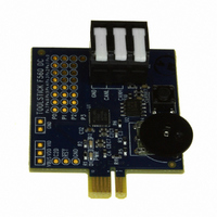
DAUGHTER CARD TOOLSTICK F560
Manufacturer
Silicon Laboratories Inc
Series
ToolStickr
Type
MCUr
Specifications of TOOLSTICK560DC
Contents
Daughter Card
Processor To Be Evaluated
C8051F55x, C8051F56x, C8051F57x
Interface Type
USB
Operating Supply Voltage
2.7 V to 3.6 V
Lead Free Status / RoHS Status
Lead free / RoHS Compliant
For Use With/related Products
C8051F55x, C8051F56x, C8051F57x
For Use With
336-1345 - TOOLSTICK BASE ADAPTER336-1182 - ADAPTER USB DEBUG FOR C8051FXXX
Lead Free Status / Rohs Status
Lead free / RoHS Compliant
Other names
336-1719


C8051F55x/56x/57x
6.2. Output Code Formatting
The registers ADC0H and ADC0L contain the high and low bytes of the output conversion code. When the
repeat count is set to 1, conversion codes are represented in 12-bit unsigned integer format and the output
conversion code is updated after each conversion. Inputs are measured from 0 to V
can be right-justified or left-justified, depending on the setting of the AD0LJST bit (ADC0CN.2). Unused
bits in the ADC0H and ADC0L registers are set to 0. Example codes are shown below for both right-justi-
fied and left-justified data.
When the ADC0 Repeat Count is greater than 1, the output conversion code represents the accumulated
result of the conversions performed and is updated after the last conversion in the series is finished. Sets
of 4, 8, or 16 consecutive samples can be accumulated and represented in unsigned integer format. The
repeat count can be selected using the AD0RPT bits in the ADC0CF register. The value must be right-jus-
tified (AD0LJST = 0), and unused bits in the ADC0H and ADC0L registers are set to 0. The following
example shows right-justified codes for repeat counts greater than 1. Notice that accumulating 2
is equivalent to left-shifting by n bit positions when all samples returned from the ADC have the same
value.
6.2.1. Settling Time Requirements
A minimum tracking time is required before an accurate conversion is performed. This tracking time is
determined by any series impedance, including the AMUX0 resistance, the ADC0 sampling capacitance,
and the accuracy required for the conversion.
Figure 6.5 shows the equivalent ADC0 input circuit. The required ADC0 settling time for a given settling
accuracy (SA) may be approximated by Equation 6.1. When measuring the Temperature Sensor output,
use the settling time specified in Table 5.10. When measuring V
R
sampling capacitor values.
Where:
SA is the settling accuracy, given as a fraction of an LSB (for example, 0.25 to settle within 1/4 LSB).
t is the required settling time in seconds. R
source resistance. n is the ADC resolution in bits (10).
52
V
V
V
MUX
REF
REF
REF
VREF x 4095/4096
VREF x 2048/4096
VREF x 2047/4096
Input Voltage
Input Voltage
. See Table 5.9 for ADC0 minimum settling time requirements as well as the mux impedance and
x 4095/4096
x 2048/4096
x 2047/4096
0
0
Repeat Count = 4
Equation 6.1. ADC0 Settling Time Requirements
Right-Justified ADC0H:ADC0L
0x3FFC
0x1FFC
0x2000
0x0000
t
=
(AD0LJST = 0)
ln
0x0FFF
------- -
SA
0x07FF
0x0800
0x0000
2
n
TOTAL
R
Rev. 1.1
Repeat Count = 8
is the sum of the AMUX0 resistance and any external
TOTAL
0x7FF8
0x3FF8
0x4000
0x0000
C
SAMPLE
DD
with respect to GND, R
Left-Justified ADC0H:ADC0L
(AD0LJST = 1)
Repeat Count = 16
0xFFF0
0x7FF0
0x8000
0x0000
REF
0xFFF0
0x7FF0
0x8000
0x0000
x 4095/4096. Data
TOTAL
reduces to
n
samples
Related parts for TOOLSTICK560DC
Image
Part Number
Description
Manufacturer
Datasheet
Request
R

Part Number:
Description:
KIT TOOL EVAL SYS IN A USB STICK
Manufacturer:
Silicon Laboratories Inc
Datasheet:

Part Number:
Description:
TOOLSTICK DEBUG ADAPTER
Manufacturer:
Silicon Laboratories Inc
Datasheet:

Part Number:
Description:
TOOLSTICK BASE ADAPTER
Manufacturer:
Silicon Laboratories Inc
Datasheet:

Part Number:
Description:
TOOLSTICK DAUGHTER CARD
Manufacturer:
Silicon Laboratories Inc
Datasheet:

Part Number:
Description:
TOOLSTICK DAUGHTER CARD
Manufacturer:
Silicon Laboratories Inc
Datasheet:

Part Number:
Description:
TOOLSTICK DAUGHTER CARD
Manufacturer:
Silicon Laboratories Inc
Datasheet:

Part Number:
Description:
TOOLSTICK PROGRAMMING ADAPTER
Manufacturer:
Silicon Laboratories Inc
Datasheet:

Part Number:
Description:
TOOLSTICK DAUGHTER CARD
Manufacturer:
Silicon Laboratories Inc
Datasheet:

Part Number:
Description:
KIT STARTER TOOLSTICK
Manufacturer:
Silicon Laboratories Inc
Datasheet:

Part Number:
Description:
KIT UNIVERSITY TOOLSTICK STARTER
Manufacturer:
Silicon Laboratories Inc
Datasheet:

Part Number:
Description:
DAUGHTER CARD TOOLSTICK F330
Manufacturer:
Silicon Laboratories Inc
Datasheet:

Part Number:
Description:
CARD DAUGHTER UNIVRSTY TOOLSTICK
Manufacturer:
Silicon Laboratories Inc
Datasheet:

Part Number:
Description:
DAUGHTER CARD TOOLSTICK F582
Manufacturer:
Silicon Laboratories Inc
Datasheet:

Part Number:
Description:
DAUGHTER CARD TOOLSTICK F500
Manufacturer:
Silicon Laboratories Inc
Datasheet:

Part Number:
Description:
DAUGHTER CARD TOOLSTICK F540
Manufacturer:
Silicon Laboratories Inc
Datasheet: