TOOLSTICK560DC Silicon Laboratories Inc, TOOLSTICK560DC Datasheet - Page 149
TOOLSTICK560DC
Manufacturer Part Number
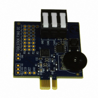
TOOLSTICK560DC
Description
DAUGHTER CARD TOOLSTICK F560
Manufacturer
Silicon Laboratories Inc
Series
ToolStickr
Type
MCUr
Specifications of TOOLSTICK560DC
Contents
Daughter Card
Processor To Be Evaluated
C8051F55x, C8051F56x, C8051F57x
Interface Type
USB
Operating Supply Voltage
2.7 V to 3.6 V
Lead Free Status / RoHS Status
Lead free / RoHS Compliant
For Use With/related Products
C8051F55x, C8051F56x, C8051F57x
For Use With
336-1345 - TOOLSTICK BASE ADAPTER336-1182 - ADAPTER USB DEBUG FOR C8051FXXX
Lead Free Status / Rohs Status
Lead free / RoHS Compliant
Other names
336-1719


17.5.3. Split Mode with Bank Select
When EMI0CF[3:2] are set to 10, the XRAM memory map is split into two areas, on-chip space and off-
chip space.
17.5.4. External Only
When EMI0CF[3:2] are set to 11, all MOVX operations are directed to off-chip space. On-chip XRAM is not
visible to the CPU. This mode is useful for accessing off-chip memory located between 0x0000 and the
internal XRAM size boundary.
17.6. Timing
The timing parameters of the External Memory Interface can be configured to enable connection to
devices having different setup and hold time requirements. The Address Setup time, Address Hold time,
RD and WR strobe widths, and in multiplexed mode, the width of the ALE pulse are all programmable in
units of SYSCLK periods through EMI0TC, shown in SFR Definition 17.3, and EMI0CF[1:0].
The timing for an off-chip MOVX instruction can be calculated by adding 4 SYSCLK cycles to the timing
parameters defined by the EMI0TC register. Assuming non-multiplexed operation, the minimum execution
time for an off-chip XRAM operation is 5 SYSCLK cycles (1 SYSCLK for RD or WR pulse + 4 SYSCLKs).
For multiplexed operations, the Address Latch Enable signal will require a minimum of 2 additional SYS-
CLK cycles. Therefore, the minimum execution time for an off-chip XRAM operation in multiplexed mode is
7 SYSCLK cycles (2 for /ALE + 1 for RD or WR + 4). The programmable setup and hold times default to
the maximum delay settings after a reset. Table 17.2 lists the ac parameters for the External Memory Inter-
face, and Figure 17.3 through Figure 17.5 show the timing diagrams for the different External Memory
Interface modes and MOVX operations.
Effective addresses below the internal XRAM size boundary will access on-chip XRAM space.
Effective addresses above the internal XRAM size boundary will access off-chip space.
8-bit MOVX operations use the contents of EMI0CN to determine whether the memory access is on-
chip or off-chip. The upper 8-bits of the Address Bus A[15:8] are determined by EMI0CN, and the lower
8-bits of the Address Bus A[7:0] are determined by R0 or R1. All 16-bits of the Address Bus A[15:0] are
driven in “Bank Select” mode.
16-bit MOVX operations use the contents of DPTR to determine whether the memory access is on-chip
or off-chip, and the full 16-bits of the Address Bus A[15:0] are driven during the off-chip transaction.
8-bit MOVX operations ignore the contents of EMI0CN. The upper Address bits A[15:8] are not driven
(identical behavior to an off-chip access in “Split Mode without Bank Select” described above). This
allows the user to manipulate the upper address bits at will by setting the Port state directly. The lower
8-bits of the effective address A[7:0] are determined by the contents of R0 or R1.
16-bit MOVX operations use the contents of DPTR to determine the effective address A[15:0]. The full
16-bits of the Address Bus A[15:0] are driven during the off-chip transaction.
Rev. 1.1
C8051F55x/56x/57x
149
Related parts for TOOLSTICK560DC
Image
Part Number
Description
Manufacturer
Datasheet
Request
R

Part Number:
Description:
KIT TOOL EVAL SYS IN A USB STICK
Manufacturer:
Silicon Laboratories Inc
Datasheet:

Part Number:
Description:
TOOLSTICK DEBUG ADAPTER
Manufacturer:
Silicon Laboratories Inc
Datasheet:

Part Number:
Description:
TOOLSTICK BASE ADAPTER
Manufacturer:
Silicon Laboratories Inc
Datasheet:

Part Number:
Description:
TOOLSTICK DAUGHTER CARD
Manufacturer:
Silicon Laboratories Inc
Datasheet:

Part Number:
Description:
TOOLSTICK DAUGHTER CARD
Manufacturer:
Silicon Laboratories Inc
Datasheet:

Part Number:
Description:
TOOLSTICK DAUGHTER CARD
Manufacturer:
Silicon Laboratories Inc
Datasheet:

Part Number:
Description:
TOOLSTICK PROGRAMMING ADAPTER
Manufacturer:
Silicon Laboratories Inc
Datasheet:

Part Number:
Description:
TOOLSTICK DAUGHTER CARD
Manufacturer:
Silicon Laboratories Inc
Datasheet:

Part Number:
Description:
KIT STARTER TOOLSTICK
Manufacturer:
Silicon Laboratories Inc
Datasheet:

Part Number:
Description:
KIT UNIVERSITY TOOLSTICK STARTER
Manufacturer:
Silicon Laboratories Inc
Datasheet:

Part Number:
Description:
DAUGHTER CARD TOOLSTICK F330
Manufacturer:
Silicon Laboratories Inc
Datasheet:

Part Number:
Description:
CARD DAUGHTER UNIVRSTY TOOLSTICK
Manufacturer:
Silicon Laboratories Inc
Datasheet:

Part Number:
Description:
DAUGHTER CARD TOOLSTICK F582
Manufacturer:
Silicon Laboratories Inc
Datasheet:

Part Number:
Description:
DAUGHTER CARD TOOLSTICK F500
Manufacturer:
Silicon Laboratories Inc
Datasheet:

Part Number:
Description:
DAUGHTER CARD TOOLSTICK F540
Manufacturer:
Silicon Laboratories Inc
Datasheet: