TOOLSTICK560DC Silicon Laboratories Inc, TOOLSTICK560DC Datasheet - Page 181
TOOLSTICK560DC
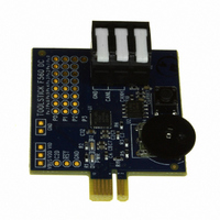
Manufacturer Part Number
TOOLSTICK560DC
Description
DAUGHTER CARD TOOLSTICK F560
Manufacturer
Silicon Laboratories Inc
Series
ToolStickr
Type
MCUr
Specifications of TOOLSTICK560DC
Contents
Daughter Card
Processor To Be Evaluated
C8051F55x, C8051F56x, C8051F57x
Interface Type
USB
Operating Supply Voltage
2.7 V to 3.6 V
Lead Free Status / RoHS Status
Lead free / RoHS Compliant
For Use With/related Products
C8051F55x, C8051F56x, C8051F57x
For Use With
336-1345 - TOOLSTICK BASE ADAPTER336-1182 - ADAPTER USB DEBUG FOR C8051FXXX
Lead Free Status / Rohs Status
Lead free / RoHS Compliant
Other names
336-1719


19.6. Special Function Registers for Accessing and Configuring Port I/O
All Port I/O are accessed through corresponding special function registers (SFRs) that are both byte
addressable and bit addressable, except for P4 which is only byte addressable. When writing to a Port, the
value written to the SFR is latched to maintain the output data value at each pin. When reading, the logic
levels of the Port's input pins are returned regardless of the XBRn settings (i.e., even when the pin is
assigned to another signal by the Crossbar, the Port register can always read its corresponding Port I/O
pin). The exception to this is the execution of the read-modify-write instructions that target a Port Latch reg-
ister as the destination. The read-modify-write instructions when operating on a Port SFR are the following:
ANL, ORL, XRL, JBC, CPL, INC, DEC, DJNZ and MOV, CLR or SETB, when the destination is an individ-
ual bit in a Port SFR. For these instructions, the value of the latch register (not the pin) is read, modified,
and written back to the SFR.
Ports 0–3 have a corresponding PnSKIP register which allows its individual Port pins to be assigned to dig-
ital functions or skipped by the Crossbar. All Port pins used for analog functions, GPIO, or dedicated digital
functions such as the EMIF should have their PnSKIP bit set to 1.
The Port input mode of the I/O pins is defined using the Port Input Mode registers (PnMDIN). Each Port
cell can be configured for analog or digital I/O. This selection is required even for the digital resources
selected in the XBRn registers, and is not automatic. The only exception to this is P4, which can only be
used for digital I/O.
The output driver characteristics of the I/O pins are defined using the Port Output Mode registers (PnMD-
OUT). Each Port Output driver can be configured as either open drain or push-pull. This selection is
required even for the digital resources selected in the XBRn registers, and is not automatic. The only
exception to this is the SMBus (SDA, SCL) pins, which are configured as open-drain regardless of the
PnMDOUT settings.
SFR Definition 19.12. P0: Port 0
SFR Address = 0x80; SFR Page = All Pages; Bit-Addressable
Name
Reset
Bit
7:0
Type
Bit
P0[7:0]
Name
7
1
Port 0 Data.
Sets the Port latch logic
value or reads the Port pin
logic state in Port cells con-
figured for digital I/O.
6
1
Description
5
1
Rev. 1.1
0: Set output latch to logic
LOW.
1: Set output latch to logic
HIGH.
4
1
P0[7:0]
R/W
Write
3
1
C8051F55x/56x/57x
2
1
0: P0.n Port pin is logic
LOW.
1: P0.n Port pin is logic
HIGH.
1
1
Read
0
1
181
Related parts for TOOLSTICK560DC
Image
Part Number
Description
Manufacturer
Datasheet
Request
R

Part Number:
Description:
KIT TOOL EVAL SYS IN A USB STICK
Manufacturer:
Silicon Laboratories Inc
Datasheet:

Part Number:
Description:
TOOLSTICK DEBUG ADAPTER
Manufacturer:
Silicon Laboratories Inc
Datasheet:

Part Number:
Description:
TOOLSTICK BASE ADAPTER
Manufacturer:
Silicon Laboratories Inc
Datasheet:

Part Number:
Description:
TOOLSTICK DAUGHTER CARD
Manufacturer:
Silicon Laboratories Inc
Datasheet:

Part Number:
Description:
TOOLSTICK DAUGHTER CARD
Manufacturer:
Silicon Laboratories Inc
Datasheet:

Part Number:
Description:
TOOLSTICK DAUGHTER CARD
Manufacturer:
Silicon Laboratories Inc
Datasheet:

Part Number:
Description:
TOOLSTICK PROGRAMMING ADAPTER
Manufacturer:
Silicon Laboratories Inc
Datasheet:

Part Number:
Description:
TOOLSTICK DAUGHTER CARD
Manufacturer:
Silicon Laboratories Inc
Datasheet:

Part Number:
Description:
KIT STARTER TOOLSTICK
Manufacturer:
Silicon Laboratories Inc
Datasheet:

Part Number:
Description:
KIT UNIVERSITY TOOLSTICK STARTER
Manufacturer:
Silicon Laboratories Inc
Datasheet:

Part Number:
Description:
DAUGHTER CARD TOOLSTICK F330
Manufacturer:
Silicon Laboratories Inc
Datasheet:

Part Number:
Description:
CARD DAUGHTER UNIVRSTY TOOLSTICK
Manufacturer:
Silicon Laboratories Inc
Datasheet:

Part Number:
Description:
DAUGHTER CARD TOOLSTICK F582
Manufacturer:
Silicon Laboratories Inc
Datasheet:

Part Number:
Description:
DAUGHTER CARD TOOLSTICK F500
Manufacturer:
Silicon Laboratories Inc
Datasheet:

Part Number:
Description:
DAUGHTER CARD TOOLSTICK F540
Manufacturer:
Silicon Laboratories Inc
Datasheet: