TOOLSTICK560DC Silicon Laboratories Inc, TOOLSTICK560DC Datasheet - Page 246
TOOLSTICK560DC
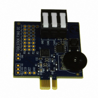
Manufacturer Part Number
TOOLSTICK560DC
Description
DAUGHTER CARD TOOLSTICK F560
Manufacturer
Silicon Laboratories Inc
Series
ToolStickr
Type
MCUr
Specifications of TOOLSTICK560DC
Contents
Daughter Card
Processor To Be Evaluated
C8051F55x, C8051F56x, C8051F57x
Interface Type
USB
Operating Supply Voltage
2.7 V to 3.6 V
Lead Free Status / RoHS Status
Lead free / RoHS Compliant
For Use With/related Products
C8051F55x, C8051F56x, C8051F57x
For Use With
336-1345 - TOOLSTICK BASE ADAPTER336-1182 - ADAPTER USB DEBUG FOR C8051FXXX
Lead Free Status / Rohs Status
Lead free / RoHS Compliant
Other names
336-1719


C8051F55x/56x/57x
24.3. SPI0 Slave Mode Operation
When SPI0 is enabled and not configured as a master, it will operate as a SPI slave. As a slave, bytes are
shifted in through the MOSI pin and out through the MISO pin by a master device controlling the SCK sig-
nal. A bit counter in the SPI0 logic counts SCK edges. When 8 bits have been shifted through the shift reg-
ister, the SPIF flag is set to logic 1, and the byte is copied into the receive buffer. Data is read from the
receive buffer by reading SPI0DAT. A slave device cannot initiate transfers. Data to be transferred to the
master device is pre-loaded into the shift register by writing to SPI0DAT. Writes to SPI0DAT are double-
buffered, and are placed in the transmit buffer first. If the shift register is empty, the contents of the transmit
buffer will immediately be transferred into the shift register. When the shift register already contains data,
the SPI will load the shift register with the transmit buffer’s contents after the last SCK edge of the next (or
current) SPI transfer.
When configured as a slave, SPI0 can be configured for 4-wire or 3-wire operation. The default, 4-wire
slave mode, is active when NSSMD1 (SPI0CN.3) = 0 and NSSMD0 (SPI0CN.2) = 1. In 4-wire mode, the
NSS signal is routed to a port pin and configured as a digital input. SPI0 is enabled when NSS is logic 0,
and disabled when NSS is logic 1. The bit counter is reset on a falling edge of NSS. Note that the NSS sig-
nal must be driven low at least 2 system clocks before the first active edge of SCK for each byte transfer.
Figure 24.4 shows a connection diagram between two slave devices in 4-wire slave mode and a master
device.
3-wire slave mode is active when NSSMD1 (SPI0CN.3) = 0 and NSSMD0 (SPI0CN.2) = 0. NSS is not
used in this mode, and is not mapped to an external port pin through the crossbar. Since there is no way of
uniquely addressing the device in 3-wire slave mode, SPI0 must be the only slave device present on the
bus. It is important to note that in 3-wire slave mode there is no external means of resetting the bit counter
that determines when a full byte has been received. The bit counter can only be reset by disabling and re-
enabling SPI0 with the SPIEN bit. Figure 24.3 shows a connection diagram between a slave device in 3-
wire slave mode and a master device.
24.4. SPI0 Interrupt Sources
When SPI0 interrupts are enabled, the following four flags will generate an interrupt when they are set to
logic 1:
All of the following bits must be cleared by software.
1. The SPI Interrupt Flag, SPIF (SPI0CN.7) is set to logic 1 at the end of each byte transfer. This flag can
2. The Write Collision Flag, WCOL (SPI0CN.6) is set to logic 1 if a write to SPI0DAT is attempted when
3. The Mode Fault Flag MODF (SPI0CN.5) is set to logic 1 when SPI0 is configured as a master, and for
4. The Receive Overrun Flag RXOVRN (SPI0CN.4) is set to logic 1 when configured as a slave, and a
246
occur in all SPI0 modes.
the transmit buffer has not been emptied to the SPI shift register. When this occurs, the write to
SPI0DAT will be ignored, and the transmit buffer will not be written.This flag can occur in all SPI0
modes.
multi-master mode and the NSS pin is pulled low. When a Mode Fault occurs, the MSTEN and SPIEN
bits in SPI0CN are set to logic 0 to disable SPI0 and allow another master device to access the bus.
transfer is completed and the receive buffer still holds an unread byte from a previous transfer. The new
byte is not transferred to the receive buffer, allowing the previously received data byte to be read. The
data byte which caused the overrun is lost.
Rev. 1.1
Related parts for TOOLSTICK560DC
Image
Part Number
Description
Manufacturer
Datasheet
Request
R

Part Number:
Description:
KIT TOOL EVAL SYS IN A USB STICK
Manufacturer:
Silicon Laboratories Inc
Datasheet:

Part Number:
Description:
TOOLSTICK DEBUG ADAPTER
Manufacturer:
Silicon Laboratories Inc
Datasheet:

Part Number:
Description:
TOOLSTICK BASE ADAPTER
Manufacturer:
Silicon Laboratories Inc
Datasheet:

Part Number:
Description:
TOOLSTICK DAUGHTER CARD
Manufacturer:
Silicon Laboratories Inc
Datasheet:

Part Number:
Description:
TOOLSTICK DAUGHTER CARD
Manufacturer:
Silicon Laboratories Inc
Datasheet:

Part Number:
Description:
TOOLSTICK DAUGHTER CARD
Manufacturer:
Silicon Laboratories Inc
Datasheet:

Part Number:
Description:
TOOLSTICK PROGRAMMING ADAPTER
Manufacturer:
Silicon Laboratories Inc
Datasheet:

Part Number:
Description:
TOOLSTICK DAUGHTER CARD
Manufacturer:
Silicon Laboratories Inc
Datasheet:

Part Number:
Description:
KIT STARTER TOOLSTICK
Manufacturer:
Silicon Laboratories Inc
Datasheet:

Part Number:
Description:
KIT UNIVERSITY TOOLSTICK STARTER
Manufacturer:
Silicon Laboratories Inc
Datasheet:

Part Number:
Description:
DAUGHTER CARD TOOLSTICK F330
Manufacturer:
Silicon Laboratories Inc
Datasheet:

Part Number:
Description:
CARD DAUGHTER UNIVRSTY TOOLSTICK
Manufacturer:
Silicon Laboratories Inc
Datasheet:

Part Number:
Description:
DAUGHTER CARD TOOLSTICK F582
Manufacturer:
Silicon Laboratories Inc
Datasheet:

Part Number:
Description:
DAUGHTER CARD TOOLSTICK F500
Manufacturer:
Silicon Laboratories Inc
Datasheet:

Part Number:
Description:
DAUGHTER CARD TOOLSTICK F540
Manufacturer:
Silicon Laboratories Inc
Datasheet: