C8051F350DK Silicon Laboratories Inc, C8051F350DK Datasheet - Page 9
C8051F350DK
Manufacturer Part Number
C8051F350DK
Description
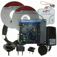
DEV KIT FOR F350/351/352/353
Manufacturer
Silicon Laboratories Inc
Type
MCUr
Specifications of C8051F350DK
Contents
Evaluation Board, Power Supply, USB Cables, Adapter and Documentation
Processor To Be Evaluated
C8051F35x
Interface Type
USB
Silicon Manufacturer
Silicon Labs
Core Architecture
8051
Silicon Core Number
C8051F350
Silicon Family Name
C8051F35x
Lead Free Status / RoHS Status
Contains lead / RoHS non-compliant
For Use With/related Products
C8051F350, 351, 352, 353
Lead Free Status / Rohs Status
Lead free / RoHS Compliant
Other names
336-1083
Available stocks
Company
Part Number
Manufacturer
Quantity
Price
Company:

Part Number:
C8051F350DK
Manufacturer:
SiliconL
Quantity:
8


22. Timers
23. Programmable Counter Array
24. Revision Specific Behavior
25. C2 Interface
Figure 22.1. T0 Mode 0 Block Diagram.................................................................. 196
Figure 22.2. T0 Mode 2 Block Diagram.................................................................. 197
Figure 22.3. T0 Mode 3 Block Diagram.................................................................. 198
Figure 22.4. Timer 2 16-Bit Mode Block Diagram .................................................. 203
Figure 22.5. Timer 2 8-Bit Mode Block Diagram .................................................... 204
Figure 22.6. Timer 3 16-Bit Mode Block Diagram .................................................. 207
Figure 22.7. Timer 3 8-Bit Mode Block Diagram .................................................... 208
Figure 23.1. PCA Block Diagram............................................................................ 211
Figure 23.2. PCA Counter/Timer Block Diagram.................................................... 212
Figure 23.3. PCA Interrupt Block Diagram ............................................................. 213
Figure 23.4. PCA Capture Mode Diagram.............................................................. 214
Figure 23.5. PCA Software Timer Mode Diagram .................................................. 215
Figure 23.6. PCA High Speed Output Mode Diagram............................................ 216
Figure 23.7. PCA Frequency Output Mode ............................................................ 217
Figure 23.8. PCA 8-Bit PWM Mode Diagram ......................................................... 218
Figure 23.9. PCA 16-Bit PWM Mode...................................................................... 219
Figure 23.10. PCA Module 2 with Watchdog Timer Enabled ................................. 220
Figure 24.1. Reading Package Marking ................................................................. 227
Figure 25.1. Typical C2 Pin Sharing....................................................................... 231
Rev. 1.1
C8051F350/1/2/3
9
Related parts for C8051F350DK
Image
Part Number
Description
Manufacturer
Datasheet
Request
R

Part Number:
Description:
SMD/C°/SINGLE-ENDED OUTPUT SILICON OSCILLATOR
Manufacturer:
Silicon Laboratories Inc
Part Number:
Description:
Manufacturer:
Silicon Laboratories Inc
Datasheet:
Part Number:
Description:
N/A N/A/SI4010 AES KEYFOB DEMO WITH LCD RX
Manufacturer:
Silicon Laboratories Inc
Datasheet:
Part Number:
Description:
N/A N/A/SI4010 SIMPLIFIED KEY FOB DEMO WITH LED RX
Manufacturer:
Silicon Laboratories Inc
Datasheet:
Part Number:
Description:
N/A/-40 TO 85 OC/EZLINK MODULE; F930/4432 HIGH BAND (REV E/B1)
Manufacturer:
Silicon Laboratories Inc
Part Number:
Description:
EZLink Module; F930/4432 Low Band (rev e/B1)
Manufacturer:
Silicon Laboratories Inc
Part Number:
Description:
I°/4460 10 DBM RADIO TEST CARD 434 MHZ
Manufacturer:
Silicon Laboratories Inc
Part Number:
Description:
I°/4461 14 DBM RADIO TEST CARD 868 MHZ
Manufacturer:
Silicon Laboratories Inc
Part Number:
Description:
I°/4463 20 DBM RFSWITCH RADIO TEST CARD 460 MHZ
Manufacturer:
Silicon Laboratories Inc
Part Number:
Description:
I°/4463 20 DBM RADIO TEST CARD 868 MHZ
Manufacturer:
Silicon Laboratories Inc
Part Number:
Description:
I°/4463 27 DBM RADIO TEST CARD 868 MHZ
Manufacturer:
Silicon Laboratories Inc
Part Number:
Description:
I°/4463 SKYWORKS 30 DBM RADIO TEST CARD 915 MHZ
Manufacturer:
Silicon Laboratories Inc
Part Number:
Description:
N/A N/A/-40 TO 85 OC/4463 RFMD 30 DBM RADIO TEST CARD 915 MHZ
Manufacturer:
Silicon Laboratories Inc
Part Number:
Description:
I°/4463 20 DBM RADIO TEST CARD 169 MHZ
Manufacturer:
Silicon Laboratories Inc