C8051F350DK Silicon Laboratories Inc, C8051F350DK Datasheet - Page 3
C8051F350DK
Manufacturer Part Number
C8051F350DK
Description
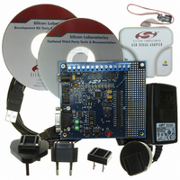
DEV KIT FOR F350/351/352/353
Manufacturer
Silicon Laboratories Inc
Type
MCUr
Specifications of C8051F350DK
Contents
Evaluation Board, Power Supply, USB Cables, Adapter and Documentation
Processor To Be Evaluated
C8051F35x
Interface Type
USB
Silicon Manufacturer
Silicon Labs
Core Architecture
8051
Silicon Core Number
C8051F350
Silicon Family Name
C8051F35x
Lead Free Status / RoHS Status
Contains lead / RoHS non-compliant
For Use With/related Products
C8051F350, 351, 352, 353
Lead Free Status / Rohs Status
Lead free / RoHS Compliant
Other names
336-1083
Available stocks
Company
Part Number
Manufacturer
Quantity
Price
Company:

Part Number:
C8051F350DK
Manufacturer:
SiliconL
Quantity:
8


Table of Contents
1. System Overview.................................................................................................... 17
2. Absolute Maximum Ratings .................................................................................. 29
3. Global DC Electrical Characteristics .................................................................... 30
4. Pinout and Package Definitions............................................................................ 31
5. 24 or 16-Bit Analog to Digital Converter (ADC0) ................................................. 41
6. 8-Bit Current Mode DACS (IDA0 and IDA1).......................................................... 67
7. Voltage Reference .................................................................................................. 73
8. Temperature Sensor............................................................................................... 77
1.1. CIP-51™ Microcontroller................................................................................... 21
1.2. On-Chip Debug Circuitry................................................................................... 22
1.3. On-Chip Memory............................................................................................... 23
1.4. 24 or 16-Bit Analog to Digital Converter (ADC0) .............................................. 24
1.5. Two 8-bit Current-Mode DACs.......................................................................... 25
1.6. Programmable Comparator .............................................................................. 26
1.7. Serial Ports ....................................................................................................... 26
1.8. Port Input/Output............................................................................................... 27
1.9. Programmable Counter Array ........................................................................... 28
5.1. Configuration..................................................................................................... 42
5.2. Calibrating the ADC .......................................................................................... 44
5.3. Performing Conversions ................................................................................... 46
5.4. Offset DAC........................................................................................................ 47
5.5. Burnout Current Sources .................................................................................. 47
5.6. Analog Multiplexer ............................................................................................ 59
6.1. IDAC Output Scheduling................................................................................... 68
6.2. IDAC Output Mapping....................................................................................... 68
6.3. IDAC External Pin Connections ........................................................................ 71
1.1.1. Fully 8051 Compatible Instruction Set...................................................... 21
1.1.2. Improved Throughput ............................................................................... 21
1.1.3. Additional Features .................................................................................. 21
5.1.1. Voltage Reference Selection.................................................................... 42
5.1.2. Analog Inputs ........................................................................................... 42
5.1.3. Modulator Clock ....................................................................................... 43
5.1.4. Decimation Ratio ...................................................................................... 43
5.2.1. Internal Calibration ................................................................................... 44
5.2.2. System Calibration ................................................................................... 44
5.2.3. Calibration Coefficient Storage................................................................. 44
5.3.1. Single Conversions .................................................................................. 46
5.3.2. Continuous Conversions .......................................................................... 46
5.3.3. ADC Output .............................................................................................. 46
5.3.4. Error Conditions ....................................................................................... 47
6.1.1. Update Output On-Demand ..................................................................... 68
6.1.2. Update Output Based on Timer Overflow ................................................ 68
6.1.3. Update Output Based on CNVSTR Edge................................................. 68
Rev. 1.1
C8051F350/1/2/3
3
Related parts for C8051F350DK
Image
Part Number
Description
Manufacturer
Datasheet
Request
R

Part Number:
Description:
SMD/C°/SINGLE-ENDED OUTPUT SILICON OSCILLATOR
Manufacturer:
Silicon Laboratories Inc
Part Number:
Description:
Manufacturer:
Silicon Laboratories Inc
Datasheet:
Part Number:
Description:
N/A N/A/SI4010 AES KEYFOB DEMO WITH LCD RX
Manufacturer:
Silicon Laboratories Inc
Datasheet:
Part Number:
Description:
N/A N/A/SI4010 SIMPLIFIED KEY FOB DEMO WITH LED RX
Manufacturer:
Silicon Laboratories Inc
Datasheet:
Part Number:
Description:
N/A/-40 TO 85 OC/EZLINK MODULE; F930/4432 HIGH BAND (REV E/B1)
Manufacturer:
Silicon Laboratories Inc
Part Number:
Description:
EZLink Module; F930/4432 Low Band (rev e/B1)
Manufacturer:
Silicon Laboratories Inc
Part Number:
Description:
I°/4460 10 DBM RADIO TEST CARD 434 MHZ
Manufacturer:
Silicon Laboratories Inc
Part Number:
Description:
I°/4461 14 DBM RADIO TEST CARD 868 MHZ
Manufacturer:
Silicon Laboratories Inc
Part Number:
Description:
I°/4463 20 DBM RFSWITCH RADIO TEST CARD 460 MHZ
Manufacturer:
Silicon Laboratories Inc
Part Number:
Description:
I°/4463 20 DBM RADIO TEST CARD 868 MHZ
Manufacturer:
Silicon Laboratories Inc
Part Number:
Description:
I°/4463 27 DBM RADIO TEST CARD 868 MHZ
Manufacturer:
Silicon Laboratories Inc
Part Number:
Description:
I°/4463 SKYWORKS 30 DBM RADIO TEST CARD 915 MHZ
Manufacturer:
Silicon Laboratories Inc
Part Number:
Description:
N/A N/A/-40 TO 85 OC/4463 RFMD 30 DBM RADIO TEST CARD 915 MHZ
Manufacturer:
Silicon Laboratories Inc
Part Number:
Description:
I°/4463 20 DBM RADIO TEST CARD 169 MHZ
Manufacturer:
Silicon Laboratories Inc