C8051F350DK Silicon Laboratories Inc, C8051F350DK Datasheet - Page 129
C8051F350DK
Manufacturer Part Number
C8051F350DK
Description
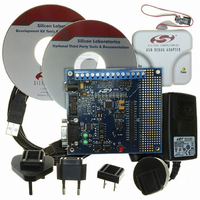
DEV KIT FOR F350/351/352/353
Manufacturer
Silicon Laboratories Inc
Type
MCUr
Specifications of C8051F350DK
Contents
Evaluation Board, Power Supply, USB Cables, Adapter and Documentation
Processor To Be Evaluated
C8051F35x
Interface Type
USB
Silicon Manufacturer
Silicon Labs
Core Architecture
8051
Silicon Core Number
C8051F350
Silicon Family Name
C8051F35x
Lead Free Status / RoHS Status
Contains lead / RoHS non-compliant
For Use With/related Products
C8051F350, 351, 352, 353
Lead Free Status / Rohs Status
Lead free / RoHS Compliant
Other names
336-1083
Available stocks
Company
Part Number
Manufacturer
Quantity
Price
Company:

Part Number:
C8051F350DK
Manufacturer:
SiliconL
Quantity:
8


17. Oscillators
C8051F350/1/2/3 devices include a programmable internal oscillator, an external oscillator drive circuit,
and a clock multiplier. The internal oscillator can be enabled/disabled and calibrated using the OSCICN
and OSCICL registers, as shown in Figure 17.1. The system clock (SYSCLK) can be derived from the
internal oscillator, external oscillator circuit, or the clock multiplier. The clock multiplier can produce three
possible outputs: Internal Oscillator x 2, External Oscillator x 2, or External Oscillator x 4. Oscillator electri-
cal specifications are given in Table 17.1 on page 136.
17.1. Programmable Internal Oscillator
All C8051F350/1/2/3 devices include a programmable internal oscillator that defaults as the system clock
after a system reset. The internal oscillator period can be programmed via the OSCICL register, shown in
SFR Definition 17.2. On C8051F350/1/2/3 devices, OSCICL is factory calibrated to obtain a 24.5 MHz fre-
quency.
Electrical specifications for the precision internal oscillator are given in Table 17.1 on page 136. Note that
the system clock may be derived from the programmed internal oscillator divided by 1, 2, 4, or 8, as
defined by the IFCN bits in register OSCICN. The divide value defaults to 8 following a reset.
VDD
Option 2
XTAL2
Option 1
Option 4
10MΩ
XTAL2
Option 3
XTAL2
XTAL1
XTAL2
Figure 17.1. Oscillator Diagram
OSCICL
Circuit
Input
Programmable
Internal Clock
Generator
OSCXCN
OSC
EN
Rev. 1.1
EXOSC / 2
OSCICN
IOSC
EXOSC
EXOSC
IOSC/2
CLKMUL
n
Clock Multiplier
x4
C8051F350/1/2/3
CLKSEL
SYSCLK
129
Related parts for C8051F350DK
Image
Part Number
Description
Manufacturer
Datasheet
Request
R

Part Number:
Description:
SMD/C°/SINGLE-ENDED OUTPUT SILICON OSCILLATOR
Manufacturer:
Silicon Laboratories Inc
Part Number:
Description:
Manufacturer:
Silicon Laboratories Inc
Datasheet:
Part Number:
Description:
N/A N/A/SI4010 AES KEYFOB DEMO WITH LCD RX
Manufacturer:
Silicon Laboratories Inc
Datasheet:
Part Number:
Description:
N/A N/A/SI4010 SIMPLIFIED KEY FOB DEMO WITH LED RX
Manufacturer:
Silicon Laboratories Inc
Datasheet:
Part Number:
Description:
N/A/-40 TO 85 OC/EZLINK MODULE; F930/4432 HIGH BAND (REV E/B1)
Manufacturer:
Silicon Laboratories Inc
Part Number:
Description:
EZLink Module; F930/4432 Low Band (rev e/B1)
Manufacturer:
Silicon Laboratories Inc
Part Number:
Description:
I°/4460 10 DBM RADIO TEST CARD 434 MHZ
Manufacturer:
Silicon Laboratories Inc
Part Number:
Description:
I°/4461 14 DBM RADIO TEST CARD 868 MHZ
Manufacturer:
Silicon Laboratories Inc
Part Number:
Description:
I°/4463 20 DBM RFSWITCH RADIO TEST CARD 460 MHZ
Manufacturer:
Silicon Laboratories Inc
Part Number:
Description:
I°/4463 20 DBM RADIO TEST CARD 868 MHZ
Manufacturer:
Silicon Laboratories Inc
Part Number:
Description:
I°/4463 27 DBM RADIO TEST CARD 868 MHZ
Manufacturer:
Silicon Laboratories Inc
Part Number:
Description:
I°/4463 SKYWORKS 30 DBM RADIO TEST CARD 915 MHZ
Manufacturer:
Silicon Laboratories Inc
Part Number:
Description:
N/A N/A/-40 TO 85 OC/4463 RFMD 30 DBM RADIO TEST CARD 915 MHZ
Manufacturer:
Silicon Laboratories Inc
Part Number:
Description:
I°/4463 20 DBM RADIO TEST CARD 169 MHZ
Manufacturer:
Silicon Laboratories Inc