C8051F350DK Silicon Laboratories Inc, C8051F350DK Datasheet - Page 232
C8051F350DK
Manufacturer Part Number
C8051F350DK
Description
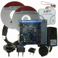
DEV KIT FOR F350/351/352/353
Manufacturer
Silicon Laboratories Inc
Type
MCUr
Specifications of C8051F350DK
Contents
Evaluation Board, Power Supply, USB Cables, Adapter and Documentation
Processor To Be Evaluated
C8051F35x
Interface Type
USB
Silicon Manufacturer
Silicon Labs
Core Architecture
8051
Silicon Core Number
C8051F350
Silicon Family Name
C8051F35x
Lead Free Status / RoHS Status
Contains lead / RoHS non-compliant
For Use With/related Products
C8051F350, 351, 352, 353
Lead Free Status / Rohs Status
Lead free / RoHS Compliant
Other names
336-1083
Available stocks
Company
Part Number
Manufacturer
Quantity
Price
Company:

Part Number:
C8051F350DK
Manufacturer:
SiliconL
Quantity:
8


•
•
C8051F350/1/2/3
D
Revision 0.4 to Revision 1.0
•
•
•
•
•
•
•
•
•
•
•
•
Revision 1.0 to Revision 1.1
•
•
•
•
•
•
•
•
•
•
•
•
•
•
232
OCUMENT
Removed preliminary tag and updated various specifications.
Updated package labeling and added "Lead-free (RoHS Compliant)" in Table 1.1, “Product Selection
Guide,” on page 18.
ADC chapter: Added Table 5.5, Table 5.6, Table 5.7, Table 5.8, and Table 5.9 on pages 63–65.
Temperature Sensor chapter: Added Offset Error and Slope Error specifications to Table 8.1, “Temper-
ature Sensor Electrical Characteristics,” on page 77.
Reset Sources chapter: Table 14.1, “Reset Electrical Characteristics,” on page 120: Added V
Time and changed “V
Flash Memory chapter: Clarified descriptions of Flash security features.
Oscillators chapter: Clarified external crystal initialization steps and added a specific 32.768 kHz crys-
tal example.
Oscillators chapter: Clarified external capacitor example.
Port I/O chapter: Figure 18.3 and Figure 18.4, Crossbar Priority Decoder Tables: Changed
PnSKIP[7:0] to PnSKIP[0:7] to match the Port I/O order.
SMBus chapter: SFR Definition 19.1, SMB0CF register: Added a description of the behavior of Timer 3
in split mode if SMBTOE is set.
PCA chapter: Updated Watchdog timer timeout intervals in Table 23.3 on page 221.
C2 chapter: Removed references to “boundary scans.”
Clarified text in Table 2.1, “Absolute Maximum Ratings,” on page 29.
Updated Digital Supply Current values in Table 3.1, “Global DC Electrical Characteristics,” on page 30.
Removed sentence in Section “5.2. Calibrating the ADC’ on page 44 that indicated the AD0CALC bit is
cleared by clearing the AD0INT flag.
Updated Table 5.3, “ADC0 Electrical Characteristics,” on page 61.
- ADC input current
- Burnout Current Source values
- AV+ Supply Current values
Added second note to SFR Definition 5.3.
Updated Table 6.1, “IDAC Electrical Characteristics,” on page 72.
- IDAC0 Gain-error Temp Co.
- IDAC0 Power consumption values
Clarified usage of VREF– pin in text and figure in 7. ‘Voltage Reference” on page 73.
Updated Table 7.1, “Voltage Reference Electrical Characteristics,” on page 75.
- VREF output voltage max and min
- Power Specifications
Corrected pins used by Comparator0 output in Section “9.1. Comparator0 Inputs and Outputs’ on
page 83.
Updated Comparator Power Consumptions values in Table 9.1, “Comparator Electrical Characteris-
tics,” on page 85.
Corrected maximum SMBus speed in Section “19. SMBus’ on page 151.
Updated Table 19.4, “SMBus Status Decoding,” on page 167.
- Slave Transmitter (0101 0XX)
- Slave Receiver (0001 00X)
Fixed Equation 23.4.
Added last step to procedure described in Section “23.3.2. Watchdog Timer Usage’ on page 221.
Changed Note 2 in Table 23.3, “Watchdog Timer Timeout Intervals1,” on page 221.
Added Section “24. Revision Specific Behavior’ on page 227.
C
HANGE
DD
POR Threshold” to “V
L
IST
Rev. 1.1
DD
Monitor Threshold.”
DD
Ramp
Related parts for C8051F350DK
Image
Part Number
Description
Manufacturer
Datasheet
Request
R

Part Number:
Description:
SMD/C°/SINGLE-ENDED OUTPUT SILICON OSCILLATOR
Manufacturer:
Silicon Laboratories Inc
Part Number:
Description:
Manufacturer:
Silicon Laboratories Inc
Datasheet:
Part Number:
Description:
N/A N/A/SI4010 AES KEYFOB DEMO WITH LCD RX
Manufacturer:
Silicon Laboratories Inc
Datasheet:
Part Number:
Description:
N/A N/A/SI4010 SIMPLIFIED KEY FOB DEMO WITH LED RX
Manufacturer:
Silicon Laboratories Inc
Datasheet:
Part Number:
Description:
N/A/-40 TO 85 OC/EZLINK MODULE; F930/4432 HIGH BAND (REV E/B1)
Manufacturer:
Silicon Laboratories Inc
Part Number:
Description:
EZLink Module; F930/4432 Low Band (rev e/B1)
Manufacturer:
Silicon Laboratories Inc
Part Number:
Description:
I°/4460 10 DBM RADIO TEST CARD 434 MHZ
Manufacturer:
Silicon Laboratories Inc
Part Number:
Description:
I°/4461 14 DBM RADIO TEST CARD 868 MHZ
Manufacturer:
Silicon Laboratories Inc
Part Number:
Description:
I°/4463 20 DBM RFSWITCH RADIO TEST CARD 460 MHZ
Manufacturer:
Silicon Laboratories Inc
Part Number:
Description:
I°/4463 20 DBM RADIO TEST CARD 868 MHZ
Manufacturer:
Silicon Laboratories Inc
Part Number:
Description:
I°/4463 27 DBM RADIO TEST CARD 868 MHZ
Manufacturer:
Silicon Laboratories Inc
Part Number:
Description:
I°/4463 SKYWORKS 30 DBM RADIO TEST CARD 915 MHZ
Manufacturer:
Silicon Laboratories Inc
Part Number:
Description:
N/A N/A/-40 TO 85 OC/4463 RFMD 30 DBM RADIO TEST CARD 915 MHZ
Manufacturer:
Silicon Laboratories Inc
Part Number:
Description:
I°/4463 20 DBM RADIO TEST CARD 169 MHZ
Manufacturer:
Silicon Laboratories Inc