P0528 Terasic Technologies Inc, P0528 Datasheet - Page 8
P0528
Manufacturer Part Number
P0528
Description
BOARD DEV DE1 ALTERA
Manufacturer
Terasic Technologies Inc
Type
FPGAr
Datasheet
1.P0528.pdf
(56 pages)
Specifications of P0528
Contents
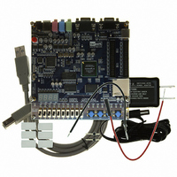
DE1 Board, Power Supply, USB Cable, Plastic cover and software
For Use With/related Products
Cyclone II 2C20
For Use With
P0033 - BOARD ADAPTER HSMC TO GPIOP0006 - BOARD ADAPTER THDB-SUMP0001 - MODULE DIGITAL CAMERA 5MP (D5M)P0307 - KIT DEV 4.3" LCD TOUCH PANEL
Lead Free Status / RoHS Status
Lead free / RoHS Compliant
Other names
DE1


2.2 Block Diagram of the DE1 Board
Figure 2.2 gives the block diagram of the DE1 board. To provide maximum flexibility for the user,
all connections are made through the Cyclone II FPGA device. Thus, the user can configure the
FPGA to implement any system design.
Following is more detailed information about the blocks in Figure 2.2:
Cyclone II 2C20 FPGA
Serial Configuration device and USB Blaster circuit
SRAM
• 18,752 LEs
• 52 M4K RAM blocks
• 240K total RAM bits
• 26 embedded multipliers
• 4 PLLs
• 315 user I/O pins
• FineLine BGA 484-pin package
• Altera’s EPCS4 Serial Configuration device
• On-board USB Blaster for programming and user API control
• JTAG and AS programming modes are supported
Figure 2.2. Block diagram of the DE1 board.
6
DE1 User Manual
Related parts for P0528
Image
Part Number
Description
Manufacturer
Datasheet
Request
R

Part Number:
Description:
MODULE DIGITAL CAMERA 5MP (D5M)
Manufacturer:
Terasic Technologies Inc
Datasheet:

Part Number:
Description:
DE2-70 CALL FOR ACADEMIC PRICING
Manufacturer:
Terasic Technologies Inc
Datasheet:

Part Number:
Description:
USB BLASTER CABLE
Manufacturer:
Terasic Technologies Inc
Datasheet:

Part Number:
Description:
BOARD ADAPTER HSMC TO GPIO
Manufacturer:
Terasic Technologies Inc
Datasheet:

Part Number:
Description:
BOARD ADAPTER THDB-SUM
Manufacturer:
Terasic Technologies Inc
Datasheet:

Part Number:
Description:
KIT DEV 4.3" LCD TOUCH PANEL
Manufacturer:
Terasic Technologies Inc
Datasheet:

Part Number:
Description:
DAUGHTER BOARD AD/DA GPIO ADA
Manufacturer:
Terasic Technologies Inc

Part Number:
Description:
DAUGHTER BOARD AD/DA HSMC ADA
Manufacturer:
Terasic Technologies Inc

Part Number:
Description:
KIT MAX II MICRO
Manufacturer:
Terasic Technologies Inc
Datasheet:

Part Number:
Description:
BOARD DEV/EDUCATION ALTERA DE0
Manufacturer:
Terasic Technologies Inc
Datasheet:

Part Number:
Description:
DE2 CALL FOR ACADEMIC PRICING
Manufacturer:
Terasic Technologies Inc

Part Number:
Description:
MODULE DIGITAL CAMERA 1.3MP
Manufacturer:
Terasic Technologies Inc
Datasheet:

Part Number:
Description:
SENSOR CMOS 1.3MEGA (FOR P0349)
Manufacturer:
Terasic Technologies Inc
Datasheet:
Part Number:
Description:
MODULE DIGITAL CAMERA 5MP (D5M)
Manufacturer:
Terasic Technologies Inc
Datasheet: