P0305 Terasic Technologies Inc, P0305 Datasheet
P0305
Specifications of P0305


Related parts for P0305


P0305 Summary of contents
Page 1
Max II Micro Kit Version 1.32 MAX® II Micro Kit User Manual Copyright © 2009 Terasic Technologies ...
Page 2
Max II Micro Kit CONTENTS C hapter 1 MAX II Micro Package ackage Contents ................................................................................................................. ssemble the MAX II Micro etting Help .........................................................................................................................3 ...
Page 3
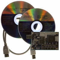
MAX II Micro Package The MAX II Micro package contains all components needed to use the MAX II Micro board in conjunction with a computer that runs the Microsoft Windows software. 1.1 P ackage Contents 0 B Figure 1.1 shows ...
Page 4
A ssemble the MAX II Micro 1 B Connect the MAX II Micro to PC either: Plug-in directly, as shown in Figure 1.2 Via the USB cable provided in the package, as shown in Figure 1.3 Figure 1.3. Connect ...
Page 5
G etting Help 2 B Here are the addresses where you can get help if you encounter problems: Altera Corporation 101 Innovation Drive San Jose, California, 95134 USA Email: u niversity@altera.com H U Terasic Technologies No. 356, Sec. 1, ...
Page 6
Altera MAX II Micro Board This chapter presents the features and design characteristics of the MAX II Micro board. 2.1 L ayout and Components photograph of the MAX II Micro board is shown in Figure 2.1. It ...
Page 7
LEDs 50-MHz oscillator for clock sources Powered by a USB cable (Type-A-Male to Type-A-Female) 2.2 B lock Diagram of the MAX II Micro Board 4 B Figure 2.2 gives the block diagram of the MAX II Micro ...
Page 8
Pushbutton switches 4 pushbutton switches Debounced by a Schmitt trigger circuit Normally high; generates one active-low pulse when the switch is pressed Clock inputs 50-MHz oscillator Prototyping Areas A 40-pin expansion port area compatible with Altera DE2/DE1 expansion ports. Prototyping ...
Page 9
A list of the pin names on the MAX II CPLD that are connected to the LEDs, pushbuttons, and clock inputs is given in Table 2.1. Signal Name LED[0] LED[1] LED[2] LED[3] LED[4] LED[5] LED[6] LED[7] KEY[0] KEY[1] KEY[2] KEY[3] ...
Page 10
Figure 2.4. Schematic diagram of the LEDs, pushbuttons, and clock circuit. 2.3.2 E xpansion Port and Prototyping Area 7 B The MAX II Micro board provides users two prototyping area: PROTO_A and PROTO_B, as shown in Figure 2.1. The schematics ...
Page 11
Figure 2.5. Schematic of the prototyping area. Figure 2.6. Schematic of the prototyping area. 9 MMK User Manual ...
Page 12
3.3 3.3V 3.3V 3.3V 3.3V GND GND GND GND GND GND Figure 2.7. The detailed I/O map of prototyping area A and B. 2.4 P ower-up the ...
Page 13
M ethods to Configure the MAX II Micro Board 9 B The MAX II Micro board provides two modes, JTAG Mode and USB Blaster Mode, which allows users to use the MAX II Micro board as a CPLD development ...
Page 14
Set the both dip switches on the Max II Micro board to UP location, as shown in Figure 2.10. 3. Connect the USB-Blaster download cable to the 10-pin header (J3) on the device board and MAX II Micro board. ...
Page 15
MAX II Micro Board Control Panel The MAX II Micro board comes with a Control Panel facility that allows users to access various components on the board through a USB connection from a host computer. This chapter first presents how ...
Page 16
Figure 3.1. Quartus II Programmer window Figure 3.2. The MAX II Micro Board Control Panel window. The concept of the MAX II Micro Control Panel is illustrated in Figure 3.3. The IP that performs the control functions is implemented in ...
Page 17
Figure 3.3. The MAX II Micro Control Panel concept. 3.2 U sing the Control Panel The interface of the MAX II Micro control panel window matches the real MAX II Micro board. Users can select the components ...
Page 18
Figure 3.4 Control panel window for LED controlling. Detection of the action of the pushbuttons When users press the pushbutton switches on the MAX II Micro board, the MAX II Micro control panel window will indicate which pushbutton switches are ...
Page 19
I/Os. Figure 3.6 Users can configure the GPIOs in the prototyping areas by clicking on the corresponding holes shown in the Control Panel window section. The GPIOs’ color will be marked by yellow to indicate their ...
Page 20
MAX II Micro Board Design This chapter demonstrates several reference designs to help users to understand how to implement their own designs using the MAX II Micro board. 4.1 D emonstration Setup mentioned in section 1.2, ...
Page 21
Figure 4.1. Set Switch1 to UP position and Switch2 to DOWN position in normal operation (JTAG 4.3 E xercise 1: Traffic Light Experiment The purpose of the exercise is to let users get familiar with logic design, ...
Page 22
State Figure 4.3 Behavior of two traffic lights at each state. Simply follow the instructions below to repeat the exercise. 1. Ensure LEDs are flashing after demonstration setup is completed. Please check connection to ...
Page 23
E xercise 2: A Color Pattern Generator Using 4.3’’ LCD Panel Users can follow the instructions below to implement a color pattern generator using a 4.3’’ touch panel with the MAX II Micro board. We are ...
Page 24
Figure 4.6. The connection setup for the 40-pin cable with MAX II Micro board. 3. Open Quartus II and locate DEN_LTM_TEST.pof under the directory \ DEN_demonstrations \ DEN_LTM_TEST \ of the CD-ROM included. 4. Download the bitstream (DEN_LTM_TEST.pof) to the ...
Page 25
Please NOTE the orientation of the 40-pin cable when connecting the DIP 40-pin male connector on the PROT_A, as shown in Figure 4.6. Figure 4.7. The connection setup for the pattern generator demo with MAX II Micro board. 3. ...
Page 26
The MAX II Micro System CD ROM contain the following directory and files: Directory name DEN_schematics DEN_demonstrations DEN_control_panel DEN_datasheet Revision History: Version V1.0 V1.1 V1.2 V1.3 V1.31 Chapter 5 Appendix Description of contents Contains the schematic of MAX II Micro ...