P0528 Terasic Technologies Inc, P0528 Datasheet - Page 22
P0528
Manufacturer Part Number
P0528
Description
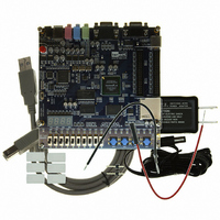
BOARD DEV DE1 ALTERA
Manufacturer
Terasic Technologies Inc
Type
FPGAr
Datasheet
1.P0528.pdf
(56 pages)
Specifications of P0528
Contents
DE1 Board, Power Supply, USB Cable, Plastic cover and software
For Use With/related Products
Cyclone II 2C20
For Use With
P0033 - BOARD ADAPTER HSMC TO GPIOP0006 - BOARD ADAPTER THDB-SUMP0001 - MODULE DIGITAL CAMERA 5MP (D5M)P0307 - KIT DEV 4.3" LCD TOUCH PANEL
Lead Free Status / RoHS Status
Lead free / RoHS Compliant
Other names
DE1


The image in Figure 3.9 is stored in an M4K memory block in the Cyclone II FPGA. It is loaded
into the M4K block in the MIF/Hex(Intel) format during the default bit stream configuration stage.
We will next describe how you can display other images and use your own images to generate the
binary data patterns that can be displayed on the VGA monitor.
Another image is provided in the file picture.dat in the folder DE1_demonstrations\pictures on the
DE1 System CD-ROM. You can display this image as follows:
• Select the SRAM page of the Control Panel and load the file picture.dat into the SRAM.
• Select the TOOLS page and choose Asynchronous 1 for the SRAM multiplexer port as
• The FPGA is now configured as indicated in Figure 3.11.
• Select the VGA page and deselect the checkbox Default Image.
• The VGA monitor should display the picture.dat image from the SRAM, as depicted in
shown in Figure 3.10. Click on the Configure button to activate the multi-port setup.
Figure 3.12. You can turn off the cursor by deselecting the Cursor Enable checkbox.
Figure 3.10. Use the Asynchronous Port 1 to access the image data in the SRAM.
20
DE1 User Manual
Related parts for P0528
Image
Part Number
Description
Manufacturer
Datasheet
Request
R

Part Number:
Description:
MODULE DIGITAL CAMERA 5MP (D5M)
Manufacturer:
Terasic Technologies Inc
Datasheet:

Part Number:
Description:
DE2-70 CALL FOR ACADEMIC PRICING
Manufacturer:
Terasic Technologies Inc
Datasheet:

Part Number:
Description:
USB BLASTER CABLE
Manufacturer:
Terasic Technologies Inc
Datasheet:

Part Number:
Description:
BOARD ADAPTER HSMC TO GPIO
Manufacturer:
Terasic Technologies Inc
Datasheet:

Part Number:
Description:
BOARD ADAPTER THDB-SUM
Manufacturer:
Terasic Technologies Inc
Datasheet:

Part Number:
Description:
KIT DEV 4.3" LCD TOUCH PANEL
Manufacturer:
Terasic Technologies Inc
Datasheet:

Part Number:
Description:
DAUGHTER BOARD AD/DA GPIO ADA
Manufacturer:
Terasic Technologies Inc

Part Number:
Description:
DAUGHTER BOARD AD/DA HSMC ADA
Manufacturer:
Terasic Technologies Inc

Part Number:
Description:
KIT MAX II MICRO
Manufacturer:
Terasic Technologies Inc
Datasheet:

Part Number:
Description:
BOARD DEV/EDUCATION ALTERA DE0
Manufacturer:
Terasic Technologies Inc
Datasheet:

Part Number:
Description:
DE2 CALL FOR ACADEMIC PRICING
Manufacturer:
Terasic Technologies Inc

Part Number:
Description:
MODULE DIGITAL CAMERA 1.3MP
Manufacturer:
Terasic Technologies Inc
Datasheet:

Part Number:
Description:
SENSOR CMOS 1.3MEGA (FOR P0349)
Manufacturer:
Terasic Technologies Inc
Datasheet:
Part Number:
Description:
MODULE DIGITAL CAMERA 5MP (D5M)
Manufacturer:
Terasic Technologies Inc
Datasheet: