P0528 Terasic Technologies Inc, P0528 Datasheet - Page 18
P0528
Manufacturer Part Number
P0528
Description
BOARD DEV DE1 ALTERA
Manufacturer
Terasic Technologies Inc
Type
FPGAr
Datasheet
1.P0528.pdf
(56 pages)
Specifications of P0528
Contents
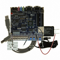
DE1 Board, Power Supply, USB Cable, Plastic cover and software
For Use With/related Products
Cyclone II 2C20
For Use With
P0033 - BOARD ADAPTER HSMC TO GPIOP0006 - BOARD ADAPTER THDB-SUMP0001 - MODULE DIGITAL CAMERA 5MP (D5M)P0307 - KIT DEV 4.3" LCD TOUCH PANEL
Lead Free Status / RoHS Status
Lead free / RoHS Compliant
Other names
DE1


To read a byte of data from a random location, enter the address of the location and click on the
Read button. The rDATA box will display the data read back from the address specified.
The Sequential Write function is used to load a file into the Flash chip as follows:
The Sequential Read function is used to read the data stored in the Flash memory and write this data
into a file as follows:
3.5 Overall Structure of the DE1 Control Panel
The DE1 Control Panel facility communicates with a circuit that is instantiated in the Cyclone II
FPGA. This circuit is specified in Verilog code, which makes it possible for a knowledgeable user
to change the functionality of the Control Panel. The code is located inside the DE1_demonstrations
directory on the DE1 System CD-ROM.
To run the Control Panel, the user must first set it up as explained in Section 3.1. Figure 3.7 depicts
the structure of the Control Panel. Each input/output device is controlled by a controller instantiated
in the FPGA chip. The communication with the PC is done via the USB Blaster link. A Command
Controller circuit interprets the commands received from the PC and performs the appropriate
actions. The SDRAM, SRAM, and Flash Memory controllers have three user-selectable
asynchronous ports in addition to the Host port that provides a link with the Command Controller.
The connection between the VGA DAC Controller and the FPGA memory allows displaying of the
default image shown on the left side of the figure, which is stored in an M4K block in the Cyclone
II chip. The connection between the Audio DAC Controller and a lookup table in the FPGA is used
to produce a test audio signal of 1 kHz.
1. Specify the starting address and the length of data (in bytes) to be written into the Flash
2. Click on the Write a File to Flash button to activate the writing process.
3. When the Control Panel responds with the standard Windows dialog box asking for the
1. Specify the starting address and the length of data (in bytes) to be read from the Flash
2. Click on the Load Flash Content to a File button to activate the reading process.
3. When the Control Panel responds with the standard Windows dialog box asking for the
memory. You can click on the File Length checkbox to indicate that you want to load the
entire file.
source file, specify the desired file in the usual manner.
memory. You can click on the Entire Flash checkbox to indicate that you want to copy the
entire contents of the Flash memory into a specified file.
destination file, specify the desired file in the usual manner.
16
DE1 User Manual
Related parts for P0528
Image
Part Number
Description
Manufacturer
Datasheet
Request
R

Part Number:
Description:
MODULE DIGITAL CAMERA 5MP (D5M)
Manufacturer:
Terasic Technologies Inc
Datasheet:

Part Number:
Description:
DE2-70 CALL FOR ACADEMIC PRICING
Manufacturer:
Terasic Technologies Inc
Datasheet:

Part Number:
Description:
USB BLASTER CABLE
Manufacturer:
Terasic Technologies Inc
Datasheet:

Part Number:
Description:
BOARD ADAPTER HSMC TO GPIO
Manufacturer:
Terasic Technologies Inc
Datasheet:

Part Number:
Description:
BOARD ADAPTER THDB-SUM
Manufacturer:
Terasic Technologies Inc
Datasheet:

Part Number:
Description:
KIT DEV 4.3" LCD TOUCH PANEL
Manufacturer:
Terasic Technologies Inc
Datasheet:

Part Number:
Description:
DAUGHTER BOARD AD/DA GPIO ADA
Manufacturer:
Terasic Technologies Inc

Part Number:
Description:
DAUGHTER BOARD AD/DA HSMC ADA
Manufacturer:
Terasic Technologies Inc

Part Number:
Description:
KIT MAX II MICRO
Manufacturer:
Terasic Technologies Inc
Datasheet:

Part Number:
Description:
BOARD DEV/EDUCATION ALTERA DE0
Manufacturer:
Terasic Technologies Inc
Datasheet:

Part Number:
Description:
DE2 CALL FOR ACADEMIC PRICING
Manufacturer:
Terasic Technologies Inc

Part Number:
Description:
MODULE DIGITAL CAMERA 1.3MP
Manufacturer:
Terasic Technologies Inc
Datasheet:

Part Number:
Description:
SENSOR CMOS 1.3MEGA (FOR P0349)
Manufacturer:
Terasic Technologies Inc
Datasheet:
Part Number:
Description:
MODULE DIGITAL CAMERA 5MP (D5M)
Manufacturer:
Terasic Technologies Inc
Datasheet: