ATSTK500 Atmel, ATSTK500 Datasheet - Page 24
ATSTK500
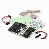
Manufacturer Part Number
ATSTK500
Description
PROGRAMMER AVR STARTER KIT
Manufacturer
Atmel
Series
AVR®r
Type
MCUr
Specifications of ATSTK500
Contents
Board, Cable, CD and Documentation
Data Bus Width
8 bit
Interface Type
RS-232
For Use With/related Products
Atmel AVR Devices
For Use With
ATADAPCAN01 - EXTENSION CAN ADD-ON TO STK500/1
Lead Free Status / RoHS Status
Lead free / RoHS Compliant


1925C–AVR–3/03
Hardware Description
3.7.2.2
3-14
Serial High-voltage
Programming
The 8-pin AVRs have too few pins to use parallel communication during High-voltage
Programming. They use serial communication instead.
This means that fewer signals have to be routed. Hardware setup for serial High-voltage
Programming is as follows:
1. Switch power off.
2. Place the device to program in its socket according to Table 3-3 on page 3-11.
3. Mount jumper OSCSEL on pins 1 and 2 to select software-controlled clock.
4. Mount jumper XTAL1 to route the oscillator signal to the device.
5. Mount jumpers VTARGET and RESET.
6. Use one 2-wire cable to connect the PB3 pin (pin 4) on the PORTB header to the
7. Use another 2-wire cable to connect the PB5 pin (pin 6) on the PORTB header to
8. Use a third 2-wire cable to connect the PB0 and PB2 pins (pins 4 and 3) on the
9. Use the last 2-wire cable to connect the PB1 pin (pin 1) on the SPROG1 header
10. Switch power on and you are ready to program.
All connections are shown in Figure 3-19.
Figure 3-19. Connection for Serial High-voltage Programming
XT1 pin (pin 7) on the PORTE/AUX header. This will connect the clock system to
the AVR device.
the RST pin (pin 4) on the PORTE/AUX header. This will connect the reset sys-
tem to the AVR device.
SPROG1 header to the DATA0 and DATA2 pins (pins 1 and 3) on the PROG
DATA header.
to the DATA1 pin (pin 2) on the PROG DATA header.
AVR STK500 User Guide
Related parts for ATSTK500
Image
Part Number
Description
Manufacturer
Datasheet
Request
R

Part Number:
Description:
DEV KIT FOR AVR/AVR32
Manufacturer:
Atmel
Datasheet:

Part Number:
Description:
INTERVAL AND WIPE/WASH WIPER CONTROL IC WITH DELAY
Manufacturer:
ATMEL Corporation
Datasheet:
Part Number:
Description:
Low-Voltage Voice-Switched IC for Hands-Free Operation
Manufacturer:
ATMEL Corporation
Datasheet:
Part Number:
Description:
MONOLITHIC INTEGRATED FEATUREPHONE CIRCUIT
Manufacturer:
ATMEL Corporation
Datasheet:
Part Number:
Description:
AM-FM Receiver IC U4255BM-M
Manufacturer:
ATMEL Corporation
Datasheet:
Part Number:
Description:
Monolithic Integrated Feature Phone Circuit
Manufacturer:
ATMEL Corporation
Datasheet:
Part Number:
Description:
Multistandard Video-IF and Quasi Parallel Sound Processing
Manufacturer:
ATMEL Corporation
Datasheet:
Part Number:
Description:
High-performance EE PLD
Manufacturer:
ATMEL Corporation
Datasheet:
Part Number:
Description:
8-bit Flash Microcontroller
Manufacturer:
ATMEL Corporation
Datasheet:
Part Number:
Description:
2-Wire Serial EEPROM
Manufacturer:
ATMEL Corporation
Datasheet: