EVL6566A-75WES4 STMicroelectronics, EVL6566A-75WES4 Datasheet - Page 7
EVL6566A-75WES4
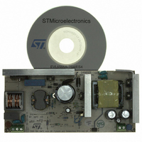
Manufacturer Part Number
EVL6566A-75WES4
Description
BOARD DEMO FOR L6563/LL6566A
Manufacturer
STMicroelectronics
Type
Power Factor Correctionr
Specifications of EVL6566A-75WES4
Main Purpose
AC/DC, Primary and Secondary Side with PFC
Outputs And Type
1, Isolated
Power - Output
75W
Voltage - Output
19V
Current - Output
4A
Voltage - Input
90 ~ 264VAC
Regulator Topology
Flyback
Board Type
Fully Populated
Utilized Ic / Part
L6563, L6566A, TSM1014
Input Voltage
90 V to 264 V
Output Voltage
19 V
Dimensions
78 mm x 170 mm
Product
Power Management Modules
Lead Free Status / RoHS Status
Lead free / RoHS Compliant
Frequency - Switching
-
Lead Free Status / Rohs Status
Lead free / RoHS Compliant
For Use With/related Products
L6563S, L6566A
Other names
497-8834
Available stocks
Company
Part Number
Manufacturer
Quantity
Price


AN2941
Operation of the “sensorless PFC” is explained as follows, referring to
Hence, properly selecting the time constant of the circuit, we can use the voltage across C
to feed the multiplier input of the L6563S because it is information about the instantaneous
value of the input voltage which is needed by the control part to shape the input current.
Figure 4.
Of course the C
to feed a stable feedback signal into the PFC controller error amplifier.
a)
where n is the winding turns ratio.
b)
c)
During the MOSFET OFF-time the voltage applied across the boost inductance is
the difference between the output and the input voltage. So D
and C
During the MOSFET ON-time the voltage applied across the boost inductor is V
(with reversed polarity) so D
D
Because C
charged is proportional to the PFC output voltage and can be used to get the
output voltage feedback signal:
2
to a voltage equal to:
Sensorless PFC operation theory
2
3
is charged via D
time constant has to be significantly longer than that of C
3
is in parallel to the series of C
Doc ID 15447 Rev 3
V
1
3
to:
=
1
V
V
is reverse biased and the capacitor C
out
2
n
=
V
−
1
V
V
=
Main characteristics and circuit description
in
out
V
+
n
n
in
−
V
V
n
in
in
1
=
and C
V
out
n
2
, the voltage at which it is
Figure 4
2
is reverse biased
1
1
and C
is charged via
:
2
in order
7/37
in
1
Related parts for EVL6566A-75WES4
Image
Part Number
Description
Manufacturer
Datasheet
Request
R

Part Number:
Description:
BOARD EVAL FOR L6566A
Manufacturer:
STMicroelectronics
Datasheet:

Part Number:
Description:
STMicroelectronics [RIPPLE-CARRY BINARY COUNTER/DIVIDERS]
Manufacturer:
STMicroelectronics
Datasheet:
Part Number:
Description:
STMicroelectronics [LIQUID-CRYSTAL DISPLAY DRIVERS]
Manufacturer:
STMicroelectronics
Datasheet:

Part Number:
Description:
BOARD EVAL FOR MEMS SENSORS
Manufacturer:
STMicroelectronics
Datasheet:
Part Number:
Description:
NPN TRANSISTOR POWER MODULE
Manufacturer:
STMicroelectronics
Datasheet:
Part Number:
Description:
TURBOSWITCH ULTRA-FAST HIGH VOLTAGE DIODE
Manufacturer:
STMicroelectronics
Datasheet:
Part Number:
Description:
Manufacturer:
STMicroelectronics
Datasheet:
Part Number:
Description:
DIODE / SCR MODULE
Manufacturer:
STMicroelectronics
Datasheet:
Part Number:
Description:
DIODE / SCR MODULE
Manufacturer:
STMicroelectronics
Datasheet:
Part Number:
Description:
Search -----> STE16N100
Manufacturer:
STMicroelectronics
Datasheet:
Part Number:
Description:
Search ---> STE53NA50
Manufacturer:
STMicroelectronics
Datasheet:
Part Number:
Description:
NPN Transistor Power Module
Manufacturer:
STMicroelectronics
Datasheet: