DTMFDECODER-RD Silicon Laboratories Inc, DTMFDECODER-RD Datasheet - Page 8
DTMFDECODER-RD
Manufacturer Part Number
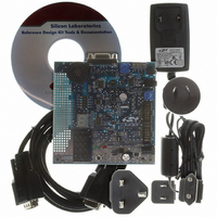
DTMFDECODER-RD
Description
KIT REF DESIGN DTMF DECODER
Manufacturer
Silicon Laboratories Inc
Specifications of DTMFDECODER-RD
Mfg Application Notes
DTMF Decoder Ref Design AppNote
Main Purpose
Telecom, DTMF Decoder
Embedded
No
Utilized Ic / Part
C8051F300
Primary Attributes
8kHz Sampling Rate ADC
Secondary Attributes
16 Goertzel Filters
Processor To Be Evaluated
C8051F300
Interface Type
RS-232
Lead Free Status / RoHS Status
Contains lead / RoHS non-compliant
Lead Free Status / RoHS Status
Lead free / RoHS Compliant, Contains lead / RoHS non-compliant
Other names
336-1283


C8051F300/1/2/3/4/5
10. Flash Memory
11. Oscillators
12. Port Input/Output
13. SMBus
14. UART0
15. Timers
16. Programmable Counter Array
17. C2 Interface
8
Figure 10.1. Flash Program Memory Map................................................................ 91
Figure 11.1. Oscillator Diagram................................................................................ 97
Figure 11.2. 32.768 kHz External Crystal Example................................................ 101
Figure 12.1. Port I/O Functional Block Diagram ..................................................... 103
Figure 12.2. Port I/O Cell Block Diagram ............................................................... 103
Figure 12.3. Crossbar Priority Decoder with XBR0 = 0x00 .................................... 104
Figure 12.4. Crossbar Priority Decoder with XBR0 = 0x44 .................................... 105
Figure 13.1. SMBus Block Diagram ....................................................................... 111
Figure 13.2. Typical SMBus Configuration ............................................................. 112
Figure 13.3. SMBus Transaction ............................................................................ 113
Figure 13.4. Typical SMBus SCL Generation......................................................... 117
Figure 13.5. Typical Master Transmitter Sequence................................................ 123
Figure 13.6. Typical Master Receiver Sequence.................................................... 124
Figure 13.7. Typical Slave Receiver Sequence...................................................... 125
Figure 13.8. Typical Slave Transmitter Sequence.................................................. 126
Figure 14.1. UART0 Block Diagram ....................................................................... 131
Figure 14.2. UART0 Baud Rate Logic .................................................................... 132
Figure 14.3. UART Interconnect Diagram .............................................................. 133
Figure 14.4. 8-Bit UART Timing Diagram............................................................... 133
Figure 14.5. 9-Bit UART Timing Diagram............................................................... 134
Figure 14.6. UART Multi-Processor Mode Interconnect Diagram .......................... 135
Figure 15.1. T0 Mode 0 Block Diagram.................................................................. 144
Figure 15.2. T0 Mode 2 Block Diagram.................................................................. 145
Figure 15.3. T0 Mode 3 Block Diagram.................................................................. 146
Figure 15.4. Timer 2 16-Bit Mode Block Diagram .................................................. 151
Figure 15.5. Timer 2 8-Bit Mode Block Diagram .................................................... 152
Figure 16.1. PCA Block Diagram............................................................................ 155
Figure 16.2. PCA Counter/Timer Block Diagram.................................................... 156
Figure 16.3. PCA Interrupt Block Diagram ............................................................. 157
Figure 16.4. PCA Capture Mode Diagram.............................................................. 158
Figure 16.5. PCA Software Timer Mode Diagram .................................................. 159
Figure 16.6. PCA High Speed Output Mode Diagram............................................ 160
Figure 16.7. PCA Frequency Output Mode ............................................................ 161
Figure 16.8. PCA 8-Bit PWM Mode Diagram ......................................................... 162
Figure 16.9. PCA 16-Bit PWM Mode...................................................................... 163
Figure 16.10. PCA Module 2 with Watchdog Timer Enabled ................................. 164
Figure 17.1. Typical C2 Pin Sharing....................................................................... 175
Rev. 2.9
Related parts for DTMFDECODER-RD
Image
Part Number
Description
Manufacturer
Datasheet
Request
R

Part Number:
Description:
SMD/C°/SINGLE-ENDED OUTPUT SILICON OSCILLATOR
Manufacturer:
Silicon Laboratories Inc
Part Number:
Description:
Manufacturer:
Silicon Laboratories Inc
Datasheet:
Part Number:
Description:
N/A N/A/SI4010 AES KEYFOB DEMO WITH LCD RX
Manufacturer:
Silicon Laboratories Inc
Datasheet:
Part Number:
Description:
N/A N/A/SI4010 SIMPLIFIED KEY FOB DEMO WITH LED RX
Manufacturer:
Silicon Laboratories Inc
Datasheet:
Part Number:
Description:
N/A/-40 TO 85 OC/EZLINK MODULE; F930/4432 HIGH BAND (REV E/B1)
Manufacturer:
Silicon Laboratories Inc
Part Number:
Description:
EZLink Module; F930/4432 Low Band (rev e/B1)
Manufacturer:
Silicon Laboratories Inc
Part Number:
Description:
I°/4460 10 DBM RADIO TEST CARD 434 MHZ
Manufacturer:
Silicon Laboratories Inc
Part Number:
Description:
I°/4461 14 DBM RADIO TEST CARD 868 MHZ
Manufacturer:
Silicon Laboratories Inc
Part Number:
Description:
I°/4463 20 DBM RFSWITCH RADIO TEST CARD 460 MHZ
Manufacturer:
Silicon Laboratories Inc
Part Number:
Description:
I°/4463 20 DBM RADIO TEST CARD 868 MHZ
Manufacturer:
Silicon Laboratories Inc
Part Number:
Description:
I°/4463 27 DBM RADIO TEST CARD 868 MHZ
Manufacturer:
Silicon Laboratories Inc
Part Number:
Description:
I°/4463 SKYWORKS 30 DBM RADIO TEST CARD 915 MHZ
Manufacturer:
Silicon Laboratories Inc
Part Number:
Description:
N/A N/A/-40 TO 85 OC/4463 RFMD 30 DBM RADIO TEST CARD 915 MHZ
Manufacturer:
Silicon Laboratories Inc
Part Number:
Description:
I°/4463 20 DBM RADIO TEST CARD 169 MHZ
Manufacturer:
Silicon Laboratories Inc