DTMFDECODER-RD Silicon Laboratories Inc, DTMFDECODER-RD Datasheet - Page 36
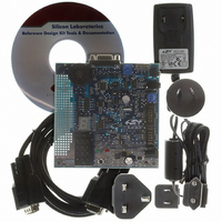
DTMFDECODER-RD
Manufacturer Part Number
DTMFDECODER-RD
Description
KIT REF DESIGN DTMF DECODER
Manufacturer
Silicon Laboratories Inc
Specifications of DTMFDECODER-RD
Mfg Application Notes
DTMF Decoder Ref Design AppNote
Main Purpose
Telecom, DTMF Decoder
Embedded
No
Utilized Ic / Part
C8051F300
Primary Attributes
8kHz Sampling Rate ADC
Secondary Attributes
16 Goertzel Filters
Processor To Be Evaluated
C8051F300
Interface Type
RS-232
Lead Free Status / RoHS Status
Contains lead / RoHS non-compliant
Lead Free Status / RoHS Status
Lead free / RoHS Compliant, Contains lead / RoHS non-compliant
Other names
336-1283


C8051F300/1/2/3/4/5
5.1.
The analog multiplexers (AMUX0) select the positive and negative inputs to the PGA, allowing any Port pin
to be measured relative to any other Port pin or GND. Additionally, the on-chip temperature sensor or the
positive power supply (V
negative input, ADC0 operates in Single-ended Mode; all other times, ADC0 operates in Differential
Mode. The ADC0 input channels are selected in the AMX0SL register as described in SFR Definition 5.1.
The conversion code format differs in Single-ended versus Differential modes, as shown below. When in
Single-ended Mode (negative input is selected GND), conversion codes are represented as 8-bit unsigned
integers. Inputs are measured from ‘0’ to VREF x 255/256. Example codes are shown below.
When in Differential Mode (negative input is not selected as GND), conversion codes are represented as
8-bit signed 2s complement numbers. Inputs are measured from –VREF to VREF x 127/128. Example
codes are shown below.
Important Note About ADC0 Input Configuration: Port pins selected as ADC0 inputs should be config-
ured as analog inputs and should be skipped by the Digital Crossbar. To configure a Port pin for analog
input, set to ‘0’ the corresponding bit in register P0MDIN. To force the Crossbar to skip a Port pin, set to ‘1’
the corresponding bit in register XBR0. See
I/O configuration details.
The PGA amplifies the AMUX0 output signal as defined by the AMP0GN1-0 bits in the ADC0 Configuration
register (SFR Definition 5.2). The PGA is software-programmable for gains of 0.5, 1, 2, or 4. The gain
defaults to 0.5 on reset.
5.2.
The typical temperature sensor transfer function is shown in Figure 5.2. The output voltage (V
positive PGA input when the temperature sensor is selected by bits AMX0P2-0 in register AMX0SL; this
voltage will be amplified by the PGA according to the user-programmed PGA settings.
36
Analog Multiplexer and PGA
Temperature Sensor
VREF x 127/128
–VREF x 64/128
VREF x 255/256
VREF x 128/256
VREF x 64/128
VREF x 64/256
Input Voltage
Input Voltage
DD
–VREF
) may be selected as the positive PGA input. When GND is selected as the
0
0
Section “12. Port Input/Output” on page 103
ADC0 Output (Conversion Code)
ADC0 Output (Conversion Code)
Rev. 2.9
0xFF
0xC0
0x80
0x40
0x00
0x7F
0x40
0x00
0x80
for more Port
TEMP
) is the
Related parts for DTMFDECODER-RD
Image
Part Number
Description
Manufacturer
Datasheet
Request
R

Part Number:
Description:
SMD/C°/SINGLE-ENDED OUTPUT SILICON OSCILLATOR
Manufacturer:
Silicon Laboratories Inc
Part Number:
Description:
Manufacturer:
Silicon Laboratories Inc
Datasheet:
Part Number:
Description:
N/A N/A/SI4010 AES KEYFOB DEMO WITH LCD RX
Manufacturer:
Silicon Laboratories Inc
Datasheet:
Part Number:
Description:
N/A N/A/SI4010 SIMPLIFIED KEY FOB DEMO WITH LED RX
Manufacturer:
Silicon Laboratories Inc
Datasheet:
Part Number:
Description:
N/A/-40 TO 85 OC/EZLINK MODULE; F930/4432 HIGH BAND (REV E/B1)
Manufacturer:
Silicon Laboratories Inc
Part Number:
Description:
EZLink Module; F930/4432 Low Band (rev e/B1)
Manufacturer:
Silicon Laboratories Inc
Part Number:
Description:
I°/4460 10 DBM RADIO TEST CARD 434 MHZ
Manufacturer:
Silicon Laboratories Inc
Part Number:
Description:
I°/4461 14 DBM RADIO TEST CARD 868 MHZ
Manufacturer:
Silicon Laboratories Inc
Part Number:
Description:
I°/4463 20 DBM RFSWITCH RADIO TEST CARD 460 MHZ
Manufacturer:
Silicon Laboratories Inc
Part Number:
Description:
I°/4463 20 DBM RADIO TEST CARD 868 MHZ
Manufacturer:
Silicon Laboratories Inc
Part Number:
Description:
I°/4463 27 DBM RADIO TEST CARD 868 MHZ
Manufacturer:
Silicon Laboratories Inc
Part Number:
Description:
I°/4463 SKYWORKS 30 DBM RADIO TEST CARD 915 MHZ
Manufacturer:
Silicon Laboratories Inc
Part Number:
Description:
N/A N/A/-40 TO 85 OC/4463 RFMD 30 DBM RADIO TEST CARD 915 MHZ
Manufacturer:
Silicon Laboratories Inc
Part Number:
Description:
I°/4463 20 DBM RADIO TEST CARD 169 MHZ
Manufacturer:
Silicon Laboratories Inc