DTMFDECODER-RD Silicon Laboratories Inc, DTMFDECODER-RD Datasheet - Page 43
DTMFDECODER-RD
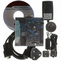
Manufacturer Part Number
DTMFDECODER-RD
Description
KIT REF DESIGN DTMF DECODER
Manufacturer
Silicon Laboratories Inc
Specifications of DTMFDECODER-RD
Mfg Application Notes
DTMF Decoder Ref Design AppNote
Main Purpose
Telecom, DTMF Decoder
Embedded
No
Utilized Ic / Part
C8051F300
Primary Attributes
8kHz Sampling Rate ADC
Secondary Attributes
16 Goertzel Filters
Processor To Be Evaluated
C8051F300
Interface Type
RS-232
Lead Free Status / RoHS Status
Contains lead / RoHS non-compliant
Lead Free Status / RoHS Status
Lead free / RoHS Compliant, Contains lead / RoHS non-compliant
Other names
336-1283


Bits7–3: AD0SC4–0: ADC0 SAR Conversion Clock Period Bits.
Bit2:
Bits1–0: AMP0GN1–0: ADC0 Internal Amplifier Gain (PGA).
Bits7–0: ADC0 Data Word.
AD0SC4
R/W
R/W
Bit7
Bit7
SFR Definition 5.2. ADC0CF: ADC0 Configuration (C8051F300/2)
SAR Conversion clock is derived from system clock by the following equation, where
AD0SC refers to the 5-bit value held in bits AD0SC4-0. SAR Conversion clock requirements
are given in Table 5.1.
UNUSED. Read = 0b; Write = don’t care.
00: Gain = 0.5
01: Gain = 1
10: Gain = 2
11: Gain = 4
ADC0 holds the output data byte from the last ADC0 conversion. When in Single-ended
mode, ADC0 holds an 8-bit unsigned integer. When in Differential mode, ADC0 holds a 2’s
complement signed 8-bit integer.
AD0SC
AD0SC3
SFR Definition 5.3. ADC0: ADC0 Data Word (C8051F300/2)
R/W
R/W
Bit6
Bit6
=
SYSCLK
--------------------- - 1
CLK
AD0SC2
R/W
R/W
Bit5
Bit5
SAR
–
AD0SC1
R/W
R/W
Bit4
Bit4
AD0SC0
Rev. 2.9
R/W
R/W
Bit3
Bit3
R/W
R/W
Bit2
Bit2
—
C8051F300/1/2/3/4/5
AMP0GN1 AMP0GN0 11111000
R/W
R/W
Bit1
Bit1
R/W
R/W
Bit0
Bit0
SFR Address:
SFR Address:
00000000
Reset Value
Reset Value
0xBE
0xBC
43
Related parts for DTMFDECODER-RD
Image
Part Number
Description
Manufacturer
Datasheet
Request
R

Part Number:
Description:
SMD/C°/SINGLE-ENDED OUTPUT SILICON OSCILLATOR
Manufacturer:
Silicon Laboratories Inc
Part Number:
Description:
Manufacturer:
Silicon Laboratories Inc
Datasheet:
Part Number:
Description:
N/A N/A/SI4010 AES KEYFOB DEMO WITH LCD RX
Manufacturer:
Silicon Laboratories Inc
Datasheet:
Part Number:
Description:
N/A N/A/SI4010 SIMPLIFIED KEY FOB DEMO WITH LED RX
Manufacturer:
Silicon Laboratories Inc
Datasheet:
Part Number:
Description:
N/A/-40 TO 85 OC/EZLINK MODULE; F930/4432 HIGH BAND (REV E/B1)
Manufacturer:
Silicon Laboratories Inc
Part Number:
Description:
EZLink Module; F930/4432 Low Band (rev e/B1)
Manufacturer:
Silicon Laboratories Inc
Part Number:
Description:
I°/4460 10 DBM RADIO TEST CARD 434 MHZ
Manufacturer:
Silicon Laboratories Inc
Part Number:
Description:
I°/4461 14 DBM RADIO TEST CARD 868 MHZ
Manufacturer:
Silicon Laboratories Inc
Part Number:
Description:
I°/4463 20 DBM RFSWITCH RADIO TEST CARD 460 MHZ
Manufacturer:
Silicon Laboratories Inc
Part Number:
Description:
I°/4463 20 DBM RADIO TEST CARD 868 MHZ
Manufacturer:
Silicon Laboratories Inc
Part Number:
Description:
I°/4463 27 DBM RADIO TEST CARD 868 MHZ
Manufacturer:
Silicon Laboratories Inc
Part Number:
Description:
I°/4463 SKYWORKS 30 DBM RADIO TEST CARD 915 MHZ
Manufacturer:
Silicon Laboratories Inc
Part Number:
Description:
N/A N/A/-40 TO 85 OC/4463 RFMD 30 DBM RADIO TEST CARD 915 MHZ
Manufacturer:
Silicon Laboratories Inc
Part Number:
Description:
I°/4463 20 DBM RADIO TEST CARD 169 MHZ
Manufacturer:
Silicon Laboratories Inc