MA240017 Microchip Technology, MA240017 Datasheet - Page 250
MA240017
Manufacturer Part Number
MA240017
Description
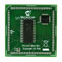
MODULE PLUG-IN PIC24F16KA102 PIM
Manufacturer
Microchip Technology
Series
PIC®r
Specifications of MA240017
Accessory Type
Plug-In Module (PIM) - PIC24F16KA102
Product
Microcontroller Modules
Data Bus Width
16 bit
Core Processor
PIC24F16KA102
Operating Supply Voltage
3 V to 3.6 V
Development Tools By Supplier
Integrated Development Environment, Assembler, ANSI C Compiler
Processor Series
PIC24F
Silicon Manufacturer
Microchip
Core Architecture
PIC
Core Sub-architecture
PIC24
Silicon Core Number
PIC24F
Silicon Family Name
PIC24FxxKAxx
Lead Free Status / RoHS Status
Lead free / RoHS Compliant
For Use With/related Products
Explorer 16 (DM240001 or DM240002)
For Use With
DM240001 - BOARD DEMO PIC24/DSPIC33/PIC32
Lead Free Status / Rohs Status
Lead free / RoHS Compliant
Available stocks
Company
Part Number
Manufacturer
Quantity
Price
Company:

Part Number:
MA240017
Manufacturer:
MICROCHIP
Quantity:
12 000


PIC24F16KA102 FAMILY
Resets
Revision History ............................................................... 243
RTCC ............................................................................... 151
S
Selective Peripheral Power Control ................................. 107
Serial Peripheral Interface. See SPI.
SFR Space ......................................................................... 28
Software Simulator (MPLAB SIM) .................................... 200
Software Stack ................................................................... 37
DS39927B-page 248
T2CON (Timer2 Control) .......................................... 116
T3CON (Timer3 Control) .......................................... 117
UxMODE (UARTx Mode) ......................................... 146
UxRXREG (UARTx Receive) ................................... 150
UxSTA (UARTx Status and Control) ........................ 148
UxTXREG (UARTx Transmit) .................................. 150
WKDYHR (RTCC Weekday and
YEAR (RTCC Year Value) ....................................... 156
Clock Source Selection .............................................. 59
Delay Times ............................................................... 60
Device Times ............................................................. 60
RCON Flags Operation .............................................. 59
SFR States ................................................................. 61
Alarm Configuration ................................................. 160
Alarm Mask Settings (figure) .................................... 161
Calibration ................................................................ 160
Register Mapping ..................................................... 152
Selecting Clock Source ............................................ 152
Source Clock ............................................................ 151
Write Lock ................................................................ 152
Hours Value) .................................................... 157
Preliminary
T
Timer1 .............................................................................. 111
Timer2/3 ........................................................................... 113
Timing Diagrams
Timing Requirements
U
UART ............................................................................... 143
Unused I/Os ....................................................................... 18
V
Voltage Regulator Pins ...................................................... 17
W
Watchdog Timer
Watchdog Timer (WDT) ................................................... 196
WWW Address ................................................................ 249
WWW, On-Line Support ...................................................... 6
CLKO and I/O Timing .............................................. 226
External Clock .......................................................... 224
CLKO and I/O .......................................................... 226
External Clock .......................................................... 224
PLL Clock Specifications ......................................... 225
Baud Rate Generator (BRG) ................................... 144
Break and Sync Transmit Sequence ....................... 145
IrDA Support ............................................................ 145
Operation of UxCTS and UxRTS Control Pins ........ 145
Receiving in 8-Bit or 9-Bit Data Mode ...................... 145
Transmitting in 8-Bit Data Mode .............................. 145
Transmitting in 9-Bit Data Mode .............................. 145
Deep Sleep (DSWDT) ............................................. 197
Windowed Operation ............................................... 196
© 2009 Microchip Technology Inc.
Related parts for MA240017
Image
Part Number
Description
Manufacturer
Datasheet
Request
R

Part Number:
Description:
Manufacturer:
Microchip Technology Inc.
Datasheet:
Part Number:
Description:
Manufacturer:
Microchip Technology Inc.
Datasheet:
Part Number:
Description:
Manufacturer:
Microchip Technology Inc.
Datasheet:
Part Number:
Description:
Manufacturer:
Microchip Technology Inc.
Datasheet:
Part Number:
Description:
Manufacturer:
Microchip Technology Inc.
Datasheet:
Part Number:
Description:
Manufacturer:
Microchip Technology Inc.
Datasheet:
Part Number:
Description:
Manufacturer:
Microchip Technology Inc.
Datasheet:
Part Number:
Description:
Manufacturer:
Microchip Technology Inc.
Datasheet: