MA240017 Microchip Technology, MA240017 Datasheet - Page 177
MA240017
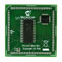
Manufacturer Part Number
MA240017
Description
MODULE PLUG-IN PIC24F16KA102 PIM
Manufacturer
Microchip Technology
Series
PIC®r
Specifications of MA240017
Accessory Type
Plug-In Module (PIM) - PIC24F16KA102
Product
Microcontroller Modules
Data Bus Width
16 bit
Core Processor
PIC24F16KA102
Operating Supply Voltage
3 V to 3.6 V
Development Tools By Supplier
Integrated Development Environment, Assembler, ANSI C Compiler
Processor Series
PIC24F
Silicon Manufacturer
Microchip
Core Architecture
PIC
Core Sub-architecture
PIC24
Silicon Core Number
PIC24F
Silicon Family Name
PIC24FxxKAxx
Lead Free Status / RoHS Status
Lead free / RoHS Compliant
For Use With/related Products
Explorer 16 (DM240001 or DM240002)
For Use With
DM240001 - BOARD DEMO PIC24/DSPIC33/PIC32
Lead Free Status / Rohs Status
Lead free / RoHS Compliant
Available stocks
Company
Part Number
Manufacturer
Quantity
Price
Company:

Part Number:
MA240017
Manufacturer:
MICROCHIP
Quantity:
12 000


REGISTER 22-5:
REGISTER 22-6:
© 2009 Microchip Technology Inc.
bit 15
bit 7
Legend:
R = Readable bit
-n = Value at POR
bit 15-13
bit 12-10
bit 9-6
bit 5-0
bit 15
bit 7
Legend:
R = Readable bit
-n = Value at POR
bit 15-13
bit 12-10
bit 9-6
bit 5-0
U-0
U-0
U-0
U-0
—
—
—
—
Unimplemented: Read as ‘0’
PCFG<12:10>: Analog Input Pin Configuration Control bits
1 = Pin for corresponding analog channel is configured in Digital mode; I/O port read enabled
0 = Pin configured in Analog mode; I/O port read disabled; A/D samples pin voltage
Unimplemented: Read as ‘0’
PCFG<5:0>: Analog Input Pin Configuration Control bits
1 = Pin for corresponding analog channel is configured in Digital mode; I/O port read enabled
0 = Pin configured in Analog mode; I/O port read disabled; A/D samples pin voltage
Unimplemented: Read as ‘0’
CSSL<12:10>: A/D Input Pin Scan Selection bits
1 = Corresponding analog channel selected for input scan
0 = Analog channel omitted from input scan
Unimplemented: Read as ‘0’
CSSL<5:0>: A/D Input Pin Scan Selection bits
1 = Corresponding analog channel selected for input scan
0 = Analog channel omitted from input scan
U-0
U-0
U-0
U-0
—
—
—
—
AD1PCFG: A/D PORT CONFIGURATION REGISTER
AD1CSSL: A/D INPUT SCAN SELECT REGISTER (LOW)
W = Writable bit
‘1’ = Bit is set
W = Writable bit
‘1’ = Bit is set
PCFG5
CSSL5
R/W-0
R/W-0
U-0
U-0
—
—
CSSL12
PCFG12
CSSL4
R/W-0
R/W-0
PCFG4
R/W-0
R/W-0
Preliminary
PIC24F16KA102 FAMILY
U = Unimplemented bit, read as ‘0’
‘0’ = Bit is cleared
U = Unimplemented bit, read as ‘0’
‘0’ = Bit is cleared
CSSL11
CSSL3
R/W-0
R/W-0
PCFG11
PCFG3
R/W-0
R/W-0
CSSL10
CSSL2
R/W-0
R/W-0
PCFG10
PCFG2
R/W-0
R/W-0
x = Bit is unknown
x = Bit is unknown
CSSL1
R/W-0
PCFG1
U-0
R/W-0
—
U-0
—
DS39927B-page 175
CSSL0
R/W-0
PCFG0
R/W-0
U-0
—
U-0
—
bit 8
bit 0
bit 8
bit 0
Related parts for MA240017
Image
Part Number
Description
Manufacturer
Datasheet
Request
R

Part Number:
Description:
Manufacturer:
Microchip Technology Inc.
Datasheet:
Part Number:
Description:
Manufacturer:
Microchip Technology Inc.
Datasheet:
Part Number:
Description:
Manufacturer:
Microchip Technology Inc.
Datasheet:
Part Number:
Description:
Manufacturer:
Microchip Technology Inc.
Datasheet:
Part Number:
Description:
Manufacturer:
Microchip Technology Inc.
Datasheet:
Part Number:
Description:
Manufacturer:
Microchip Technology Inc.
Datasheet:
Part Number:
Description:
Manufacturer:
Microchip Technology Inc.
Datasheet:
Part Number:
Description:
Manufacturer:
Microchip Technology Inc.
Datasheet: