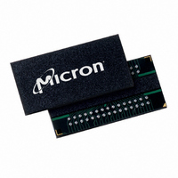
MT41J64M16LA-187E:B TR Micron Technology Inc, MT41J64M16LA-187E:B TR Datasheet - Page 58

MT41J64M16LA-187E:B TR
Manufacturer Part Number
MT41J64M16LA-187E:B TR
Description
IC DDR3 SDRAM 1GBIT 96FBGA
Manufacturer
Micron Technology Inc
Type
DDR3 SDRAMr
Specifications of MT41J64M16LA-187E:B TR
Format - Memory
RAM
Memory Type
DDR3 SDRAM
Memory Size
1G (64M x 16)
Speed
533MHz
Interface
Parallel
Voltage - Supply
1.425 V ~ 1.575 V
Operating Temperature
0°C ~ 95°C
Package / Case
96-FBGA
Organization
64Mx16
Density
1Gb
Address Bus
16b
Maximum Clock Rate
1.066GHz
Operating Supply Voltage (typ)
1.5V
Package Type
FBGA
Operating Temp Range
0C to 95C
Operating Supply Voltage (max)
1.575V
Operating Supply Voltage (min)
1.425V
Supply Current
265mA
Pin Count
96
Mounting
Surface Mount
Operating Temperature Classification
Commercial
Lead Free Status / RoHS Status
Lead free / RoHS Compliant
Other names
557-1378-2
- Current page: 58 of 181
- Download datasheet (9Mb)
Table 44:
Output Characteristics and Operating Conditions
Table 45:
PDF: 09005aef826aa906/Source: 09005aef82a357c3
1Gb_DDR3_3.fm - Rev. F 11/08 EN
Parameter/Condition
Output leakage current: DQ are disabled;
0V ≤ V
Output slew rate: Single-ended; For rising and falling
edges, measure between V
V
Single-ended DC high-level output voltage
Single-ended DC mid-point level output voltage
Single-ended DC low-level output voltage
Single-ended AC high-level output voltage
Single-ended AC low-level output voltage
Delta R
Test load for AC timing and output slew rates
OH
(
AC
OUT
) = V
ON
≤ V
between pull-up and pull-down for DQ/DQS
REF
DD
40Ω Output Driver Voltage and Temperature Sensitivity
Single-Ended Output Driver Characteristics
All voltages are referenced to Vss
+ 0.1 × V
Q; ODT is disabled; ODT is HIGH
Notes:
DD
Q
OL
The DRAM uses both single-ended and differential output drivers. The single-ended
output driver is summarized in Table 45 while the differential output driver is summa-
rized in Table 46 on page 59.
1. RZQ of 240Ω (±1 percent) with RZQ/7 enabled (default 34Ω driver) and is applicable after
2. V
3. See Figure 32 on page 60 for the test load configuration.
4. See Table 35 on page 55 for IV curve linearity. Do not use AC test load.
5. See Table 47 on page 61 for output slew rate.
6. See Table 35 on page 55 for additional information.
7. See Figure 30 on page 59 for an example of a single-ended output signal.
(
AC
proper ZQ calibration has been performed at a stable temperature and voltage
(V
) = V
TT
DD
= V
Q = V
REF
dR
dR
dR
dR
dR
dR
Change
DD
ON
ON
ON
ON
- 0.1 × V
ON
ON
Q/2.
DD
dVM
dTM
dVH
dTH
dVL
dTL
, V
SS
DD
Q = V
Q and
Output Characteristics and Operating Conditions
SS
).
Symbol
MM
V
V
V
58
V
V
SRQ
OM
OH
OH
OL
OL
I
OZ
PUPD
(
(
Min
(
(
(
DC
AC
DC
AC
SE
DC
0
0
0
0
0
0
Output to V
)
)
)
)
)
Micron Technology, Inc., reserves the right to change products or specifications without notice.
Min
–10
2.5
–5
TT
V
V
1Gb: x4, x8, x16 DDR3 SDRAM
TT
TT
(V
0.8 × V
0.5 × V
0.2 × V
+ 0.1 × V
Max
- 0.1 × V
0.15
0.15
0.15
DD
1.5
1.5
1.5
Q/2) via 25Ω resistor
DD
DD
DD
Q
Q
Q
DD
DD
Q
Max
Q
+10
+5
©2006 Micron Technology, Inc. All rights reserved.
5
%/mV
%/mV
%/mV
Units
%/°C
%/°C
%/°C
Unit
V/ns
µA
%
V
V
V
V
V
1, 2, 3, 5
1, 2, 3, 5
Notes
1, 2, 3
1, 2, 4
1, 2, 4
1, 2, 4
1, 6
1
3
Related parts for MT41J64M16LA-187E:B TR
Image
Part Number
Description
Manufacturer
Datasheet
Request
R

Part Number:
Description:
IC DDR3 SDRAM 1GBIT 96FBGA
Manufacturer:
Micron Technology Inc
Datasheet:

Part Number:
Description:
Manufacturer:
Micron Technology Inc
Datasheet:

Part Number:
Description:
Manufacturer:
Micron Technology Inc
Datasheet:

Part Number:
Description:
Manufacturer:
Micron Technology Inc
Datasheet:

Part Number:
Description:
IC SDRAM 64MBIT 133MHZ 54TSOP
Manufacturer:
Micron Technology Inc
Datasheet:

Part Number:
Description:
IC SDRAM 64MBIT 5.5NS 86TSOP
Manufacturer:
Micron Technology Inc
Datasheet:

Part Number:
Description:
IC SDRAM 64MBIT 200MHZ 86TSOP
Manufacturer:
Micron Technology Inc
Datasheet:

Part Number:
Description:
IC SDRAM 64MBIT 133MHZ 54TSOP
Manufacturer:
Micron Technology Inc
Datasheet:

Part Number:
Description:
IC SDRAM 128MBIT 133MHZ 54TSOP
Manufacturer:
Micron Technology Inc
Datasheet:

Part Number:
Description:
IC SDRAM 256MBIT 133MHZ 90VFBGA
Manufacturer:
Micron Technology Inc
Datasheet:

Part Number:
Description:
IC SDRAM 128MBIT 133MHZ 54TSOP
Manufacturer:
Micron Technology Inc
Datasheet:

Part Number:
Description:
IC SDRAM 256MBIT 133MHZ 54TSOP
Manufacturer:
Micron Technology Inc
Datasheet:

Part Number:
Description:
IC DDR SDRAM 512MBIT 6NS 66TSOP
Manufacturer:
Micron Technology Inc
Datasheet:

Part Number:
Description:
IC SDRAM 128MBIT 167MHZ 86TSOP
Manufacturer:
Micron Technology Inc
Datasheet:

Part Number:
Description:
IC SDRAM 128MBIT 143MHZ 86TSOP
Manufacturer:
Micron Technology Inc
Datasheet:


