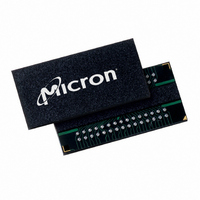
MT41J64M16LA-187E:B TR Micron Technology Inc, MT41J64M16LA-187E:B TR Datasheet - Page 137

MT41J64M16LA-187E:B TR
Manufacturer Part Number
MT41J64M16LA-187E:B TR
Description
IC DDR3 SDRAM 1GBIT 96FBGA
Manufacturer
Micron Technology Inc
Type
DDR3 SDRAMr
Specifications of MT41J64M16LA-187E:B TR
Format - Memory
RAM
Memory Type
DDR3 SDRAM
Memory Size
1G (64M x 16)
Speed
533MHz
Interface
Parallel
Voltage - Supply
1.425 V ~ 1.575 V
Operating Temperature
0°C ~ 95°C
Package / Case
96-FBGA
Organization
64Mx16
Density
1Gb
Address Bus
16b
Maximum Clock Rate
1.066GHz
Operating Supply Voltage (typ)
1.5V
Package Type
FBGA
Operating Temp Range
0C to 95C
Operating Supply Voltage (max)
1.575V
Operating Supply Voltage (min)
1.425V
Supply Current
265mA
Pin Count
96
Mounting
Surface Mount
Operating Temperature Classification
Commercial
Lead Free Status / RoHS Status
Lead free / RoHS Compliant
Other names
557-1378-2
- Current page: 137 of 181
- Download datasheet (9Mb)
Figure 80: Data Strobe Timing – READs
Figure 81: Method for Calculating
PDF: 09005aef826aa906/Source: 09005aef82a357c3
1Gb_DDR3_4.fm - Rev. F 11/08 EN
early strobe
DQS, DQS#
DQS, DQS#
late strobe
CK#
CK
t HZ (DQS), t HZ (DQ)
t LZ (DQS) MIN
t HZ (DQS), t HZ (DQ) end point = 2 × T1 - T2
Notes:
T0
t LZ (DQS) MAX
t RPRE
t
parameters are referenced to a specific voltage level which specifies when the device
output is no longer driving
t
driving
signal at two different voltages. The actual voltage measurement points are not critical
as long as the calculation is consistent. The parameters
and
1. Within a burst, the rising strobe edge is not necessarily fixed at
2. The DQS high pulse width is defined by
3. The minimum pulse width of the READ preamble is defined by
HZ and
LZ (DQ). Figure 81 shows a method to calculate the point when the device is no longer
t DQSCK (MIN)
(MAX). Instead, the rising strobe edge can vary between
t
case) and
case); however, they tend to track one another.
pulse width of the READ postamble is defined by
QSL. Likewise,
t
HZ (DQ) are defined as single-ended.
t RPRE
Bit 0
RL measured
to this point
t
HZ (DQS) and
t
LZ transitions occur in the same access time as valid data transitions. These
T1
T1
t QSH
t DQSCK (MAX)
t
LZ (DQS) MAX and
T2
Bit 0
t
Bit 1
LZ and
t
t QSH
LZ (DQS) MIN and
t DQSCK (MIN)
t QSL
Bit 1
V
V
V
V
Bit 2
OH
OH
OL
OL
t
t
HZ (DQ) or begins driving
HZ
+ 2xmV
+ xmV
t QSL
- xmV
- 2xmV
T2
t QSH
t DQSCK (MAX)
t
HZ (DQS) and
Bit 2
137
Bit 3
t
HZ (DQS) MAX are not tied to
t QSH
t DQSCK (MIN)
t QSL
t
HZ (DQS) MIN are not tied to
Bit 4
Bit 3
V
Micron Technology, Inc., reserves the right to change products or specifications without notice.
V
V
TT
t QSL
V
t
TT
QSH, and the DQS low pulse width is defined by
T3
TT
TT
+ 2xmV
t DQSCK (MAX)
- 2xmV
t
+ xmV
t LZ (DQS), t LZ (DQ) begin point = 2 × T1 - T2
HZ (DQ) or begins driving
- xmV
Bit 4
Bit 5
1Gb: x4, x8, x16 DDR3 SDRAM
t DQSCK (MIN)
t
RPST (MIN).
t
LZ (DQS),
Bit 5
Bit 6
T1
t
t
T2
LZ (DQS),
T4
DQSCK (MIN) and
t DQSCK (MAX)
Bit 6
t
Bit 7
DQSCK (MAX) (late strobe
t
LZ (DQ) by measuring the
t
t
©2006 Micron Technology, Inc. All rights reserved.
RPRE (MIN). The minimum
t
t LZ (DQS), t LZ (DQ)
DQSCK (MIN) or
t HZ (DQS) MIN
DQSCK (MIN) (early strobe
t RPST
t
LZ (DQ),
Bit 7
t
t RPST
LZ (DQS),
T5
t HZ (DQS) MAX
t
Operations
DQSCK (MAX).
t
HZ (DQS),
t
DQSCK
T6
Related parts for MT41J64M16LA-187E:B TR
Image
Part Number
Description
Manufacturer
Datasheet
Request
R

Part Number:
Description:
IC DDR3 SDRAM 1GBIT 96FBGA
Manufacturer:
Micron Technology Inc
Datasheet:

Part Number:
Description:
Manufacturer:
Micron Technology Inc
Datasheet:

Part Number:
Description:
Manufacturer:
Micron Technology Inc
Datasheet:

Part Number:
Description:
Manufacturer:
Micron Technology Inc
Datasheet:

Part Number:
Description:
IC SDRAM 64MBIT 133MHZ 54TSOP
Manufacturer:
Micron Technology Inc
Datasheet:

Part Number:
Description:
IC SDRAM 64MBIT 5.5NS 86TSOP
Manufacturer:
Micron Technology Inc
Datasheet:

Part Number:
Description:
IC SDRAM 64MBIT 200MHZ 86TSOP
Manufacturer:
Micron Technology Inc
Datasheet:

Part Number:
Description:
IC SDRAM 64MBIT 133MHZ 54TSOP
Manufacturer:
Micron Technology Inc
Datasheet:

Part Number:
Description:
IC SDRAM 128MBIT 133MHZ 54TSOP
Manufacturer:
Micron Technology Inc
Datasheet:

Part Number:
Description:
IC SDRAM 256MBIT 133MHZ 90VFBGA
Manufacturer:
Micron Technology Inc
Datasheet:

Part Number:
Description:
IC SDRAM 128MBIT 133MHZ 54TSOP
Manufacturer:
Micron Technology Inc
Datasheet:

Part Number:
Description:
IC SDRAM 256MBIT 133MHZ 54TSOP
Manufacturer:
Micron Technology Inc
Datasheet:

Part Number:
Description:
IC DDR SDRAM 512MBIT 6NS 66TSOP
Manufacturer:
Micron Technology Inc
Datasheet:

Part Number:
Description:
IC SDRAM 128MBIT 167MHZ 86TSOP
Manufacturer:
Micron Technology Inc
Datasheet:

Part Number:
Description:
IC SDRAM 128MBIT 143MHZ 86TSOP
Manufacturer:
Micron Technology Inc
Datasheet:


