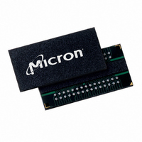
MT41J64M16LA-187E:B TR Micron Technology Inc, MT41J64M16LA-187E:B TR Datasheet - Page 109

MT41J64M16LA-187E:B TR
Manufacturer Part Number
MT41J64M16LA-187E:B TR
Description
IC DDR3 SDRAM 1GBIT 96FBGA
Manufacturer
Micron Technology Inc
Type
DDR3 SDRAMr
Specifications of MT41J64M16LA-187E:B TR
Format - Memory
RAM
Memory Type
DDR3 SDRAM
Memory Size
1G (64M x 16)
Speed
533MHz
Interface
Parallel
Voltage - Supply
1.425 V ~ 1.575 V
Operating Temperature
0°C ~ 95°C
Package / Case
96-FBGA
Organization
64Mx16
Density
1Gb
Address Bus
16b
Maximum Clock Rate
1.066GHz
Operating Supply Voltage (typ)
1.5V
Package Type
FBGA
Operating Temp Range
0C to 95C
Operating Supply Voltage (max)
1.575V
Operating Supply Voltage (min)
1.425V
Supply Current
265mA
Pin Count
96
Mounting
Surface Mount
Operating Temperature Classification
Commercial
Lead Free Status / RoHS Status
Lead free / RoHS Compliant
Other names
557-1378-2
- Current page: 109 of 181
- Download datasheet (9Mb)
Figure 53: MRS-to-nonMRS Command Timing (
Mode Register 0 (MR0)
Burst Length
PDF: 09005aef826aa906/Source: 09005aef82a357c3
1Gb_DDR3_4.fm - Rev. F 11/08 EN
Notes:
1. Prior to issuing the MRS command, all banks must be idle (they must be precharged,
2. Prior to Ta2 when
3. If R
4. CKE must be registered HIGH from the MRS command until
The base register, MR0, is used to define various DDR3 SDRAM modes of operation.
These definitions include the selection of a burst length, burst type, CAS latency, oper-
ating mode, DLL RESET, write recovery, and precharge power-down mode, as shown in
Figure 54 on page 110.
Burst length is defined by MR0[1: 0] (see Figure 54 on page 110). Read and write accesses
to the DDR3 SDRAM are burst-oriented, with the burst length being programmable to
“4” (chop mode), “8” (fixed), or selectable using A12 during a READ/WRITE command
(on-the-fly). The burst length determines the maximum number of column locations
that can be accessed for a given READ or WRITE command. When MR0[1:0] is set to “01”
during a READ/WRITE command, if A12 = 0, then BC4 (chop) mode is selected. If
A12 = 1, then BL8 mode is selected. Specific timing diagrams, and turnaround between
READ/WRITE, are shown in the READ/WRITE sections of this document.
When a READ or WRITE command is issued, a block of columns equal to the burst
length is effectively selected. All accesses for that burst take place within this block,
meaning that the burst will wrap within the block if a boundary is reached. The block is
uniquely selected by A[i:2] when the burst length is set to “4” and by A[i:3] when the
burst length is set to “8” (where Ai is the most significant column address bit for a given
configuration). The remaining (least significant) address bit(s) is (are) used to select the
starting location within the block. The programmed burst length applies to both READ
and WRITE bursts.
Command
Address
must be satisfied, and no data bursts can be in progress).
issued.
prior to Ta1. ODT must also be registered LOW at each rising CK edge from T0 until
t
power-down may occur (see "Power-Down Mode" on page 151).
MOD (MIN) is satisfied at Ta2.
CKE
CK#
TT
CK
was previously enabled, ODT must be registered LOW at T0 so that ODTL is satisfied
setting
Old
Valid
MRS
T0
t
MOD (MIN) is being satisfied, no commands (except NOP/DES) may be
NOP
t
T1
MOD)
109
Micron Technology, Inc., reserves the right to change products or specifications without notice.
NOP
T2
Updating setting
t MOD
1Gb: x4, x8, x16 DDR3 SDRAM
NOP
Ta0
t
MRSPDEN (MIN), at which time
Indicates A Break in
Time Scale
©2006 Micron Technology, Inc. All rights reserved.
NOP
Ta1
Operations
Don’t Care
Valid
Valid
MRS
non
Ta2
t
setting
RP
New
Related parts for MT41J64M16LA-187E:B TR
Image
Part Number
Description
Manufacturer
Datasheet
Request
R

Part Number:
Description:
IC DDR3 SDRAM 1GBIT 96FBGA
Manufacturer:
Micron Technology Inc
Datasheet:

Part Number:
Description:
Manufacturer:
Micron Technology Inc
Datasheet:

Part Number:
Description:
Manufacturer:
Micron Technology Inc
Datasheet:

Part Number:
Description:
Manufacturer:
Micron Technology Inc
Datasheet:

Part Number:
Description:
IC SDRAM 64MBIT 133MHZ 54TSOP
Manufacturer:
Micron Technology Inc
Datasheet:

Part Number:
Description:
IC SDRAM 64MBIT 5.5NS 86TSOP
Manufacturer:
Micron Technology Inc
Datasheet:

Part Number:
Description:
IC SDRAM 64MBIT 200MHZ 86TSOP
Manufacturer:
Micron Technology Inc
Datasheet:

Part Number:
Description:
IC SDRAM 64MBIT 133MHZ 54TSOP
Manufacturer:
Micron Technology Inc
Datasheet:

Part Number:
Description:
IC SDRAM 128MBIT 133MHZ 54TSOP
Manufacturer:
Micron Technology Inc
Datasheet:

Part Number:
Description:
IC SDRAM 256MBIT 133MHZ 90VFBGA
Manufacturer:
Micron Technology Inc
Datasheet:

Part Number:
Description:
IC SDRAM 128MBIT 133MHZ 54TSOP
Manufacturer:
Micron Technology Inc
Datasheet:

Part Number:
Description:
IC SDRAM 256MBIT 133MHZ 54TSOP
Manufacturer:
Micron Technology Inc
Datasheet:

Part Number:
Description:
IC DDR SDRAM 512MBIT 6NS 66TSOP
Manufacturer:
Micron Technology Inc
Datasheet:

Part Number:
Description:
IC SDRAM 128MBIT 167MHZ 86TSOP
Manufacturer:
Micron Technology Inc
Datasheet:

Part Number:
Description:
IC SDRAM 128MBIT 143MHZ 86TSOP
Manufacturer:
Micron Technology Inc
Datasheet:


