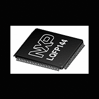
LPC2926_27_29 NXP Semiconductors, LPC2926_27_29 Datasheet - Page 64

LPC2926_27_29
Manufacturer Part Number
LPC2926_27_29
Description
The LPC2926/2927/2929 combine an ARM968E-S CPU core with two integrated TCMblocks operating at frequencies of up to 125 MHz, Full-speed USB 2
Manufacturer
NXP Semiconductors
Datasheet
1.LPC2926_27_29.pdf
(95 pages)
- Current page: 64 of 95
- Download datasheet (2Mb)
NXP Semiconductors
Table 34.
V
T
specified.
LPC2926_27_29
Product data sheet
Symbol
V
V
I
I
I
I
C
Output pins and I/O pins configured as output
V
V
V
C
USB pins USB_D+ and USB_D−
Input characteristics
V
V
V
Output characteristics
Z
V
V
I
LIH
LIL
I(pd)
I(pu)
OH
vj
DD(CORE)
o
IL
hys
O
OH
OL
IH
IL
hys
OH
OL
i
L
=
−
40
°
[1]
C to +85
= V
Static characteristics
DD(OSC_PLL)
Parameter
LOW-level input voltage
hysteresis voltage
HIGH-level input leakage
current
LOW-level input leakage
current
pull-down input current
pull-up input current
input capacitance
output voltage
HIGH-level output voltage I
LOW-level output voltage I
load capacitance
HIGH-level input voltage
LOW-level input voltage
hysteresis voltage
output impedance
HIGH-level output voltage (driven) for
LOW-level output voltage (driven) for
HIGH-level output current at V
°
C; all voltages are measured with respect to ground; positive currents flow into the IC; unless otherwise
; V
DD(IO)
= 2.7 V to 3.6 V; V
…continued
All information provided in this document is subject to legal disclaimers.
with 33 Ω series resistor
Conditions
all port pins, RST, TRST,
TDI, JTAGSEL, TMS,
TCK
all port pins, V
V
all port pins, RST, TRST,
TDI, JTAGSEL, TMS:
V
allowed
low-/full-speed; R
15 kΩ to GND
low-/full-speed; with
1.5 kΩ resistor to 3.6 V
external pull-up
without 33 Ω external
series resistor
at V
with 33 Ω external series
resistor
OH
OL
I
I
= 5.5 V
= 0 V; V
= 4 mA
= −4 mA
OH
OH
Rev. 5 — 28 September 2010
= V
= V
DDA(ADC3V3)
I
DD(IO)
DD(IO)
> 3.6 V is not
I
= 3.3 V;
− 0.3 V;
− 0.3 V;
L
of
= 3.0 V to 3.6 V; V
ARM9 microcontroller with CAN, LIN, and USB
[7]
Min
-
0.4
-
-
25
−25
-
0
V
-
-
1.5
-
0.4
2.9
-
20.8
4.8
36.0
DD(IO)
LPC2926/2927/2929
DDA(ADC5V0)
− 0.4
Typ
-
-
-
-
50
−50
3
-
-
-
-
-
-
-
-
-
-
-
-
= 3.0 V to 5.5 V;
V
25
-
1.3
Max
0.8
-
1
1
100
−115
8
-
0.4
-
44.1
3.5
0.18
41.7
5.3
DD(IO)
© NXP B.V. 2010. All rights reserved.
64 of 95
Unit
V
V
μA
μA
μA
μA
pF
V
V
V
pF
V
V
V
Ω
V
V
mA
mA
Related parts for LPC2926_27_29
Image
Part Number
Description
Manufacturer
Datasheet
Request
R
Part Number:
Description:
Lpc2926/2927/2929 Arm9 Microcontroller With Can, Lin, And Usb
Manufacturer:
NXP Semiconductors
Datasheet:
Part Number:
Description:
NXP Semiconductors designed the LPC2420/2460 microcontroller around a 16-bit/32-bitARM7TDMI-S CPU core with real-time debug interfaces that include both JTAG andembedded trace
Manufacturer:
NXP Semiconductors
Datasheet:

Part Number:
Description:
NXP Semiconductors designed the LPC2458 microcontroller around a 16-bit/32-bitARM7TDMI-S CPU core with real-time debug interfaces that include both JTAG andembedded trace
Manufacturer:
NXP Semiconductors
Datasheet:
Part Number:
Description:
NXP Semiconductors designed the LPC2468 microcontroller around a 16-bit/32-bitARM7TDMI-S CPU core with real-time debug interfaces that include both JTAG andembedded trace
Manufacturer:
NXP Semiconductors
Datasheet:
Part Number:
Description:
NXP Semiconductors designed the LPC2470 microcontroller, powered by theARM7TDMI-S core, to be a highly integrated microcontroller for a wide range ofapplications that require advanced communications and high quality graphic displays
Manufacturer:
NXP Semiconductors
Datasheet:
Part Number:
Description:
NXP Semiconductors designed the LPC2478 microcontroller, powered by theARM7TDMI-S core, to be a highly integrated microcontroller for a wide range ofapplications that require advanced communications and high quality graphic displays
Manufacturer:
NXP Semiconductors
Datasheet:
Part Number:
Description:
The Philips Semiconductors XA (eXtended Architecture) family of 16-bit single-chip microcontrollers is powerful enough to easily handle the requirements of high performance embedded applications, yet inexpensive enough to compete in the market for hi
Manufacturer:
NXP Semiconductors
Datasheet:
Part Number:
Description:
The XA-S3 device is a member of Philips Semiconductors? XA(eXtended Architecture) family of high performance 16-bitsingle-chip microcontrollers
Manufacturer:
NXP Semiconductors
Datasheet:

Part Number:
Description:
The NXP BlueStreak LH75401/LH75411 family consists of two low-cost 16/32-bit System-on-Chip (SoC) devices
Manufacturer:
NXP Semiconductors
Datasheet:

Part Number:
Description:
The NXP LPC3130/3131 combine an 180 MHz ARM926EJ-S CPU core, high-speed USB2
Manufacturer:
NXP Semiconductors
Datasheet:

Part Number:
Description:
The NXP LPC3141 combine a 270 MHz ARM926EJ-S CPU core, High-speed USB 2
Manufacturer:
NXP Semiconductors

Part Number:
Description:
The NXP LPC3143 combine a 270 MHz ARM926EJ-S CPU core, High-speed USB 2
Manufacturer:
NXP Semiconductors

Part Number:
Description:
The NXP LPC3152 combines an 180 MHz ARM926EJ-S CPU core, High-speed USB 2
Manufacturer:
NXP Semiconductors

Part Number:
Description:
The NXP LPC3154 combines an 180 MHz ARM926EJ-S CPU core, High-speed USB 2
Manufacturer:
NXP Semiconductors


