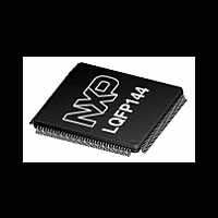
LPC2926_27_29 NXP Semiconductors, LPC2926_27_29 Datasheet - Page 50

LPC2926_27_29
Manufacturer Part Number
LPC2926_27_29
Description
The LPC2926/2927/2929 combine an ARM968E-S CPU core with two integrated TCMblocks operating at frequencies of up to 125 MHz, Full-speed USB 2
Manufacturer
NXP Semiconductors
Datasheet
1.LPC2926_27_29.pdf
(95 pages)
- Current page: 50 of 95
- Download datasheet (2Mb)
NXP Semiconductors
LPC2926_27_29
Product data sheet
6.16.2.1 Functional description
6.16.2 Clock Generation Unit (CGU0)
The key features are:
Remark: Any clock-frequency adjustment has a direct impact on the timing of all on-board
peripherals.
The clock generation unit provides 11 internal clock sources as described in
Table 27.
[1]
[2]
For generation of these base clocks, the CGU consists of primary and secondary clock
generators and one output generator for each base clock.
Number Name
0
1
2
3
4
5
6
7
8
9
10
11
•
•
•
•
•
•
•
•
•
Generation of 11 base clocks, selectable from several embedded clock sources.
Crystal oscillator with power-down.
Control PLL with power-down.
Very low-power ring oscillator, always on to provide a safe clock.
Individual source selector for each base clock, with glitch-free switching.
Autonomous clock-activity detection on every clock source.
Protection against switching to invalid or inactive clock sources.
Embedded frequency counter.
Register write-protection mechanism to prevent unintentional alteration of clocks.
Maximum frequency that guarantees stable operation of the LPC2926/2927/2929.
Fixed to low-power oscillator.
BASE_SAFE_CLK
BASE_SYS_CLK
BASE_PCR_CLK
BASE_IVNSS_CLK
BASE_MSCSS_CLK
BASE_ICLK0_CLK
BASE_UART_CLK
BASE_SPI_CLK
BASE_TMR_CLK
BASE_ADC_CLK
reserved
BASE_ICLK1_CLK
CGU0 base clocks
All information provided in this document is subject to legal disclaimers.
Rev. 5 — 28 September 2010
-
Frequency
(MHz)
0.4
125
0.4
125
125
125
125
50
125
4.5
125
ARM9 microcontroller with CAN, LIN, and USB
[2]
[1]
LPC2926/2927/2929
-
Description
base safe clock (always on)
base system clock
base PCR subsystem clock
base IVNSS subsystem clock
base MSCSS subsystem clock
base internal clock 0, for CGU1
base UART clock
base SPI clock
base timers clock
base ADCs clock
base internal clock 1, for CGU1
© NXP B.V. 2010. All rights reserved.
Table
27.
50 of 95
Related parts for LPC2926_27_29
Image
Part Number
Description
Manufacturer
Datasheet
Request
R
Part Number:
Description:
Lpc2926/2927/2929 Arm9 Microcontroller With Can, Lin, And Usb
Manufacturer:
NXP Semiconductors
Datasheet:
Part Number:
Description:
NXP Semiconductors designed the LPC2420/2460 microcontroller around a 16-bit/32-bitARM7TDMI-S CPU core with real-time debug interfaces that include both JTAG andembedded trace
Manufacturer:
NXP Semiconductors
Datasheet:

Part Number:
Description:
NXP Semiconductors designed the LPC2458 microcontroller around a 16-bit/32-bitARM7TDMI-S CPU core with real-time debug interfaces that include both JTAG andembedded trace
Manufacturer:
NXP Semiconductors
Datasheet:
Part Number:
Description:
NXP Semiconductors designed the LPC2468 microcontroller around a 16-bit/32-bitARM7TDMI-S CPU core with real-time debug interfaces that include both JTAG andembedded trace
Manufacturer:
NXP Semiconductors
Datasheet:
Part Number:
Description:
NXP Semiconductors designed the LPC2470 microcontroller, powered by theARM7TDMI-S core, to be a highly integrated microcontroller for a wide range ofapplications that require advanced communications and high quality graphic displays
Manufacturer:
NXP Semiconductors
Datasheet:
Part Number:
Description:
NXP Semiconductors designed the LPC2478 microcontroller, powered by theARM7TDMI-S core, to be a highly integrated microcontroller for a wide range ofapplications that require advanced communications and high quality graphic displays
Manufacturer:
NXP Semiconductors
Datasheet:
Part Number:
Description:
The Philips Semiconductors XA (eXtended Architecture) family of 16-bit single-chip microcontrollers is powerful enough to easily handle the requirements of high performance embedded applications, yet inexpensive enough to compete in the market for hi
Manufacturer:
NXP Semiconductors
Datasheet:
Part Number:
Description:
The XA-S3 device is a member of Philips Semiconductors? XA(eXtended Architecture) family of high performance 16-bitsingle-chip microcontrollers
Manufacturer:
NXP Semiconductors
Datasheet:

Part Number:
Description:
The NXP BlueStreak LH75401/LH75411 family consists of two low-cost 16/32-bit System-on-Chip (SoC) devices
Manufacturer:
NXP Semiconductors
Datasheet:

Part Number:
Description:
The NXP LPC3130/3131 combine an 180 MHz ARM926EJ-S CPU core, high-speed USB2
Manufacturer:
NXP Semiconductors
Datasheet:

Part Number:
Description:
The NXP LPC3141 combine a 270 MHz ARM926EJ-S CPU core, High-speed USB 2
Manufacturer:
NXP Semiconductors

Part Number:
Description:
The NXP LPC3143 combine a 270 MHz ARM926EJ-S CPU core, High-speed USB 2
Manufacturer:
NXP Semiconductors

Part Number:
Description:
The NXP LPC3152 combines an 180 MHz ARM926EJ-S CPU core, High-speed USB 2
Manufacturer:
NXP Semiconductors

Part Number:
Description:
The NXP LPC3154 combines an 180 MHz ARM926EJ-S CPU core, High-speed USB 2
Manufacturer:
NXP Semiconductors


