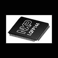
LPC2926_27_29 NXP Semiconductors, LPC2926_27_29 Datasheet - Page 40

LPC2926_27_29
Manufacturer Part Number
LPC2926_27_29
Description
The LPC2926/2927/2929 combine an ARM968E-S CPU core with two integrated TCMblocks operating at frequencies of up to 125 MHz, Full-speed USB 2
Manufacturer
NXP Semiconductors
Datasheet
1.LPC2926_27_29.pdf
(95 pages)
- Current page: 40 of 95
- Download datasheet (2Mb)
NXP Semiconductors
LPC2926_27_29
Product data sheet
Fig 8.
PAUSE
Modulation and Sampling Control SubSystem (MSCSS) block diagram
MSCSS
TIMER0
TIMER1
MSCSS
MSCSS
QEI
All information provided in this document is subject to legal disclaimers.
PWM0 TRAP
PWM0 CAP[2:0]
carrier
carrier
carrier
carrier
start
start
AHB-TO-APB BRIDGE
start
Rev. 5 — 28 September 2010
start
PWM1 TRAP
PWM1 CAP[2:0]
ADC0
PWM0
ADC1
PWM2 TRAP
synch
PWM2 CAP[2:0]
PWM1
synch
ADC2
synch
PWM3 TRAP
PWM3 CAP[2:0]
ARM9 microcontroller with CAN, LIN, and USB
synch
PWM2
synch
PWM3
LPC2926/2927/2929
IDX0
PHA0
PHB0
ADC0 IN[7:0]
ADC1 IN[7:0]
ADC2 IN[7:0]
ADC2 EXT START
PWM0 MAT[5:0]
PWM1 MAT[5:0]
PWM2 MAT[5:0]
PWM3 MAT[5:0]
© NXP B.V. 2010. All rights reserved.
002aae243
40 of 95
Related parts for LPC2926_27_29
Image
Part Number
Description
Manufacturer
Datasheet
Request
R
Part Number:
Description:
Lpc2926/2927/2929 Arm9 Microcontroller With Can, Lin, And Usb
Manufacturer:
NXP Semiconductors
Datasheet:
Part Number:
Description:
NXP Semiconductors designed the LPC2420/2460 microcontroller around a 16-bit/32-bitARM7TDMI-S CPU core with real-time debug interfaces that include both JTAG andembedded trace
Manufacturer:
NXP Semiconductors
Datasheet:

Part Number:
Description:
NXP Semiconductors designed the LPC2458 microcontroller around a 16-bit/32-bitARM7TDMI-S CPU core with real-time debug interfaces that include both JTAG andembedded trace
Manufacturer:
NXP Semiconductors
Datasheet:
Part Number:
Description:
NXP Semiconductors designed the LPC2468 microcontroller around a 16-bit/32-bitARM7TDMI-S CPU core with real-time debug interfaces that include both JTAG andembedded trace
Manufacturer:
NXP Semiconductors
Datasheet:
Part Number:
Description:
NXP Semiconductors designed the LPC2470 microcontroller, powered by theARM7TDMI-S core, to be a highly integrated microcontroller for a wide range ofapplications that require advanced communications and high quality graphic displays
Manufacturer:
NXP Semiconductors
Datasheet:
Part Number:
Description:
NXP Semiconductors designed the LPC2478 microcontroller, powered by theARM7TDMI-S core, to be a highly integrated microcontroller for a wide range ofapplications that require advanced communications and high quality graphic displays
Manufacturer:
NXP Semiconductors
Datasheet:
Part Number:
Description:
The Philips Semiconductors XA (eXtended Architecture) family of 16-bit single-chip microcontrollers is powerful enough to easily handle the requirements of high performance embedded applications, yet inexpensive enough to compete in the market for hi
Manufacturer:
NXP Semiconductors
Datasheet:
Part Number:
Description:
The XA-S3 device is a member of Philips Semiconductors? XA(eXtended Architecture) family of high performance 16-bitsingle-chip microcontrollers
Manufacturer:
NXP Semiconductors
Datasheet:

Part Number:
Description:
The NXP BlueStreak LH75401/LH75411 family consists of two low-cost 16/32-bit System-on-Chip (SoC) devices
Manufacturer:
NXP Semiconductors
Datasheet:

Part Number:
Description:
The NXP LPC3130/3131 combine an 180 MHz ARM926EJ-S CPU core, high-speed USB2
Manufacturer:
NXP Semiconductors
Datasheet:

Part Number:
Description:
The NXP LPC3141 combine a 270 MHz ARM926EJ-S CPU core, High-speed USB 2
Manufacturer:
NXP Semiconductors

Part Number:
Description:
The NXP LPC3143 combine a 270 MHz ARM926EJ-S CPU core, High-speed USB 2
Manufacturer:
NXP Semiconductors

Part Number:
Description:
The NXP LPC3152 combines an 180 MHz ARM926EJ-S CPU core, High-speed USB 2
Manufacturer:
NXP Semiconductors

Part Number:
Description:
The NXP LPC3154 combines an 180 MHz ARM926EJ-S CPU core, High-speed USB 2
Manufacturer:
NXP Semiconductors


