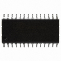
CS8420-CSZ Cirrus Logic Inc, CS8420-CSZ Datasheet - Page 13

CS8420-CSZ
Manufacturer Part Number
CS8420-CSZ
Description
IC SAMPLE RATE CONVERTER 28SOIC
Manufacturer
Cirrus Logic Inc
Type
Sample Rate Converterr
Specifications of CS8420-CSZ
Package / Case
28-SOIC
Applications
CD-R, DAT, DVD, MD, VTR
Mounting Type
Surface Mount
Operating Supply Voltage
5 V
Operating Temperature Range
- 10 C to + 70 C
Mounting Style
SMD/SMT
Resolution
17 bit to 24 bit
Control Interface
3 Wire, Serial
Supply Voltage Range
4.75V To 5.25V
Audio Ic Case Style
SOIC
No. Of Pins
28
Bandwidth
20kHz
Rohs Compliant
Yes
Audio Control Type
Volume
Dc
0841
Lead Free Status / RoHS Status
Lead free / RoHS Compliant
For Use With
598-1782 - EVALUATION BOARD FOR CS8420
Lead Free Status / Rohs Status
Lead free / RoHS Compliant
Other names
598-1125-5
Available stocks
Company
Part Number
Manufacturer
Quantity
Price
Company:
Part Number:
CS8420-CSZ
Manufacturer:
CIRRUS
Quantity:
319
Company:
Part Number:
CS8420-CSZ
Manufacturer:
CIRRUS
Quantity:
9 908
Part Number:
CS8420-CSZ
Manufacturer:
CIRRUS
Quantity:
20 000
Company:
Part Number:
CS8420-CSZ/D1
Manufacturer:
CIRRUS
Quantity:
378
Company:
Part Number:
CS8420-CSZR
Manufacturer:
NICHICON
Quantity:
4 200
direct 256*Fsi clock input via the RMCK pin, in-
stead of the PLL.
Figure 9 shows audio data entering via the AES3
Receiver. The PLL locks onto the pre-ambles in the
incoming audio stream, and generates a 256*Fsi
clock. The rate converted data is then output via the
serial audio output port and via the AES3 transmit-
ter.
Figure 10 shows the same data flow as Figure 7.
The input clock is derived from an incoming AES3
data stream. The incoming data must be synchro-
nous to the AES3 data stream.
Figure 11 shows the same data flow as Figure 7.
The input data must be synchronous to OMCK.
The output data is clocked by the recovered PLL
DS245PP2
Figure 7. Serial Audio Input, using PLL, SRC enabled
ILRCK
ISCLK
SDIN
RXN
RXP
Data Flow Control Bits
Data Flow Control Bits
Figure 9. AES3 Input, SRC enabled
TXD1-0:
SPD1-0:
SRCD:
TXD1-0:
SPD1-0:
SRCD:
Serial
Audio
Input
PLL
AES3
Rx &
Decode
PLL
00
00
0
RMCK
00
00
1
RMCK
Sample
Rate
Converter
Sample
Rate
Converter
OMCK
Clock Source Control Bits
OMCK
Clock Source Control Bits
OUTC:
INC:
RXD1-0:
OUTC:
INC:
RXD1-0:
AES3
Encoder
& Driver
Serial
Audio
Output
AES3
Encoder
& Driver
Serial
Audio
Output
0
0
00
0
0
01
OLRCK
OSCLK
SDOUT
TXP
TXN
OLRCK
OSCLK
SDOUT
TXP
TXN
clock from an AES3 input stream. This may be
used to implement a “house sync” architecture.
Figure 8 shows audio data entering via the AES3
receiver, passing through the sample rate converter,
and then exiting via the serial audio output port.
Synchronous audio data may then be input via the
serial audio input port and output via the AES3
transmitter.
Figure 13 is the same as Figure 12, but without the
sample rate converter. The whole data path is
clocked via the PLL generated recovered clock.
Figure 14 illustrates a standard AES3 receiver
function, with no rate conversion.
Figure 15 shows a standard AES3 transmitter func-
tion, with no rate conversion.
Figure 8. Serial Audio Input, No PLL, SRC enabled
ILRCK
ISCLK
SDIN
Figure 10. Serial Audio Input, AES3 Input Clock
ISCLK
ILRCK
SDIN
RXN
RXP
Data Flow Control Bits
Data Flow Control Bits
TXD1-0:
SPD1-0:
SRCD:
Serial
Audio
Input
TXD1-0:
SPD1-0:
SRCD:
AES3
Rx
Serial
Audio
Input
00
00
0
RMCK
Sample
Rate
Converter
PLL
00
00
0
RMCK OMCK
Sample
Rate
Converter
OMCK
Clock Source Control Bits
OUTC:
INC:
RXD1-0:
Clock Source Control Bits
OUTC:
INC:
RXD1-0:
AES3
Encoder
& Driver
Serial
Audio
Output
AES3
Encoder
& Driver
Serial
Audio
Output
0
0
10
0
0
01
OLRCK
OSCLK
SDOUT
TXP
TXN
CS8420
OLRCK
OSCLK
SDOUT
TXP
TXN
13


