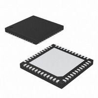
DS3510T+T&R Maxim Integrated Products, DS3510T+T&R Datasheet - Page 8

DS3510T+T&R
Manufacturer Part Number
DS3510T+T&R
Description
IC I2C GAMMA/VCOM BUFF 48-TQFN
Manufacturer
Maxim Integrated Products
Datasheet
1.DS3510TTR.pdf
(17 pages)
Specifications of DS3510T+T&R
Applications
TFT-LCD Panels: Gamma Buffer, VCOM Driver
Output Type
Rail-to-Rail
Number Of Circuits
10
Current - Supply
6.7mA
Current - Output / Channel
4mA
Voltage - Supply, Single/dual (±)
9 V ~ 15 V
Mounting Type
Surface Mount
Package / Case
48-TQFN Exposed Pad
Lead Free Status / RoHS Status
Lead free / RoHS Compliant
I
8
GM6–GM10
2
GHM, GHH
GM1–GM5
GLL, GLM
VRH, VRL
_______________________________________________________________________________________
NAME
C Gamma and V
V
V
GND
GND
SDA
N.C.
V
SCL
V
COM
LD
A0
S1
S0
CAP
DD
CC
1, 19, 20, 24
12–17, 23,
2, 38, 40,
36, 37,
42, 43
10, 11
44–48
21, 22
25–29
31–35
41, 39
PIN
EP
18
30
3
4
5
6
7
8
9
Input/Output I
Reference
Reference
Reference
Output
Output
Output
TYPE
Power
Power
Power
Input
Input
Input
Input
Input
Input
Input
Input
—
—
Analog Supply (9.0V to 15.5V)
Ground
Latch Data Input. When LD is low, Latch B retains existing data (acts as a latch).
When LD is high, the input to Latch B data flows through to the output and updates
the DACs asynchronously.
Select Inputs. When Control register [1,0] = 00, S0 and S1 pins are used to select
DAC input data from EEPROM.
I
Address Input. This pin determines I
Digital Supply (2.7V to 5.5V)
V
No Connection
Compensation Capacitor Input. Connect VCAP to GND through a 0.1μF capacitor.
References for Low-Voltage Gamma DAC
Low-Voltage Gamma Analog Outputs
V
High-Voltage Gamma Analog Outputs
References for High-Voltage Gamma DAC
Ground. Exposed pad. Connect to GND.
2
2
COM
COM
C Serial Clock Input
C Serial Data Input/Output
COM
Reference Inputs. High-voltage reference for V
Analog Output. This output requires a 1μF capacitor to GND.
Buffer with EEPROM
2
FUNCTION
C slave address of the DS3510.
COM
Pin Description
DAC.


