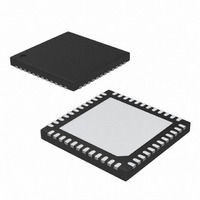
DS3510T+T&R Maxim Integrated Products, DS3510T+T&R Datasheet - Page 2

DS3510T+T&R
Manufacturer Part Number
DS3510T+T&R
Description
IC I2C GAMMA/VCOM BUFF 48-TQFN
Manufacturer
Maxim Integrated Products
Datasheet
1.DS3510TTR.pdf
(17 pages)
Specifications of DS3510T+T&R
Applications
TFT-LCD Panels: Gamma Buffer, VCOM Driver
Output Type
Rail-to-Rail
Number Of Circuits
10
Current - Supply
6.7mA
Current - Output / Channel
4mA
Voltage - Supply, Single/dual (±)
9 V ~ 15 V
Mounting Type
Surface Mount
Package / Case
48-TQFN Exposed Pad
Lead Free Status / RoHS Status
Lead free / RoHS Compliant
ABSOLUTE MAXIMUM RATINGS
Voltage on V
Voltage on VRL, VRH, GHH, GHM, GLM, GLL
Voltage on V
Voltage on SDA, SCL, A0, LD, S0,
I
RECOMMENDED OPERATING CONDITIONS
(T
INPUT ELECTRICAL CHARACTERISTICS
(V
Stresses beyond those listed under “Absolute Maximum Ratings” may cause permanent damage to the device. These are stress ratings only, and functional
operation of the device at these or any other conditions beyond those indicated in the operational sections of the specifications is not implied. Exposure to
absolute maximum rating conditions for extended periods may affect device reliability.
2
Digital Supply Voltage
Analog Supply Voltage
VRH, VRL Voltage
GHH, GHM, GLM, GLL Voltage
Input Logic 1
(SCL, SDA, A0, S0, S1, LD)
Input Logic 0
(SCL, SDA, A0, S0, S1, LD)
V
V
Input Leakage (SDA, SCL, S0,
S1, LD)
Input Leakage (A0)
V
V
Read or Write
V
V
I/O Capacitance (SDA, SCL, A0)
End-to-End Resistance
(VRH to VRL)
Relative to GND........-0.5V to (V
S1 Relative to GND ....-0.5V to (V
2
A
CC
COM
CAP
DD
CC
CC
DD
= -45°C to +95°C.)
_______________________________________________________________________________________
C Gamma and V
= +2.7V to +5.5V, T
Supply Current
Supply Current, Nonvolatile
Standby Supply Current
Standby Supply Current
Compensation Capacitor
Load Capacitor
PARAMETER
PARAMETER
DD
CC
Relative to GND ............................-0.5V to +16V
Relative to GND ..............................-0.5V to +6V
A
= -45°C to +95°C, unless otherwise noted.)
DD
CC
+ 0.5V), not to exceed 16V
SYMBOL
SYMBOL
+ 0.5V), not to exceed 6V
V
R
C
V
GM1–10
I
I
I
TOTAL
VCOM
COMP
C
V
V
CCQ
DDQ
V
L:A0
I
I
V
C
DD
CC
I
CC
DD
I/O
IH
L
IL
D
(Notes 2, 3)
(Note 4)
(Note 5)
(Note 6)
(Note 7)
COM
(Note 1)
(Note 1)
Applies to V
Applies to GM1–GM10
COM
Buffer with EEPROM
CONDITIONS
CONDITIONS
output
Junction Temperature ......................................................+125°C
Operating Temperature Range ...........................-45°C to +95°C
Programming Temperature Range .........................0°C to +70°C
Storage Temperature Range .............................-55°C to +125°C
Soldering Temperature...............Refer to IPC/JEDEC J-STD-020
GND +
0.7 x
+2.7
+9.0
+2.0
MIN
V
-0.3
MIN
0.2
0.1
-1
CC
1
TYP
TYP
6.7
0.2
1.8
16
2
5
0.3 x V
V
V
DD
DD
+15.0
+ 0.3
MAX
+5.5
V
MAX
15.0
10.0
CC
1.0
+1
10
- 2.0
- 0.2
2
4
Specification.
CC
UNITS
UNITS
mA
mA
mA
mA
μA
μA
k
μF
μF
pF
V
V
V
V
V
V


