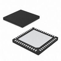
DS3510T+T&R Maxim Integrated Products, DS3510T+T&R Datasheet - Page 4

DS3510T+T&R
Manufacturer Part Number
DS3510T+T&R
Description
IC I2C GAMMA/VCOM BUFF 48-TQFN
Manufacturer
Maxim Integrated Products
Datasheet
1.DS3510TTR.pdf
(17 pages)
Specifications of DS3510T+T&R
Applications
TFT-LCD Panels: Gamma Buffer, VCOM Driver
Output Type
Rail-to-Rail
Number Of Circuits
10
Current - Supply
6.7mA
Current - Output / Channel
4mA
Voltage - Supply, Single/dual (±)
9 V ~ 15 V
Mounting Type
Surface Mount
Package / Case
48-TQFN Exposed Pad
Lead Free Status / RoHS Status
Lead free / RoHS Compliant
I
I
(V
4
2
SCL Clock Frequency
Bus Free Time Between STOP
and START Conditions
Hold Time (Repeated) START
Condition
Low Period of SCL
High Period of SCL
Data Hold Time
Data Setup Time
START Setup Time
SDA and SCL Rise Time
SDA and SCL Fall Time
STOP Setup Time
SDA and SCL Capacitive
Loading
EEPROM Write Time
Pulse-Width Suppression Time
at SDA and SCL Inputs
A0 Setup Time
A0 Hold Time
SDA and SCL Input Buffer
Hysteresis
Low-Level Output Voltage (SDA)
SCL Falling Edge to SDA Output
Data Valid
Output Data Hold
2
CC
C ELECTRICAL CHARACTERISTICS (See Figure 4)
_______________________________________________________________________________________
C Gamma and V
= +2.7V to +5.5V, T
PARAMETER
A
= -45°C to +95°C, timing referenced to V
SYMBOL
t
t
t
t
t
HD:STA
HD:DAT
SU:STO
SU:DAT
SU:STA
t
t
t
t
f
t
HIGH
SU:A
HD:A
V
LOW
t
t
SCL
BUF
C
t
t
AA
DH
t
t
W
IN
OL
R
F
B
(Note 13)
(Note 14)
(Note 14)
(Note 14)
(Note 15)
(Note 16)
Before START
After STOP
4mA sink current
SCL falling through 0.3V
0.3V
SCL falling through 0.3V
0.3V
COM
CC
CC
~0.7V
~0.7V
Buffer with EEPROM
CC
CC
CONDITIONS
window
window
IL(MAX)
CC
CC
and V
to SDA exit
until SDA in
IH(MIN)
.)
0.05 x
0.1C
0.1C
20 +
20 +
MIN
100
V
1.3
0.6
1.3
0.6
0.6
0.6
0.6
0.6
0
0
CC
0
B
B
TYP
MAX
400
300
300
400
900
0.4
0.9
20
50
UNITS
kHz
ms
pF
μs
μs
μs
μs
μs
ns
μs
ns
ns
μs
ns
μs
μs
ns
ns
V
V


