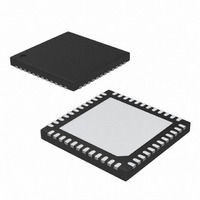
DS3510T+T&R Maxim Integrated Products, DS3510T+T&R Datasheet

DS3510T+T&R
Specifications of DS3510T+T&R
Related parts for DS3510T+T&R
DS3510T+T&R Summary of contents
Page 1
... SDA, SCL LATCH A INTERFACE A0 S1/ S0 LOGIC LD ________________________________________________________________ Maxim Integrated Products For pricing, delivery, and ordering information, please contact Maxim Direct at 1-888-629-4642, or visit Maxim’s website at www.maxim-ic.com. Buffer with EEPROM COM volt- ♦ 8-Bit Gamma Buffers, 10 Channels COM ♦ 8-Bit V COM data in on- COM ♦ ...
Page 2
I C Gamma and V ABSOLUTE MAXIMUM RATINGS Voltage on V Relative to GND ............................-0.5V to +16V DD Voltage on VRL, VRH, GHH, GHM, GLM, GLL Relative to GND........-0. 0.5V), not to exceed 16V DD Voltage ...
Page 3
I C Gamma and V INPUT ELECTRICAL CHARACTERISTICS (continued +2.7V to +5.5V -45°C to +95°C, unless otherwise noted PARAMETER SYMBOL R Tolerance TOTAL Input Resistance (GHH, GHM, GLM, GLL) Input Resistance Tolerance OUTPUT ...
Page 4
I C Gamma and ELECTRICAL CHARACTERISTICS (See Figure +2.7V to +5.5V -45°C to +95°C, timing referenced PARAMETER SYMBOL SCL Clock Frequency Bus Free Time Between STOP ...
Page 5
I C Gamma and V NONVOLATILE MEMORY CHARACTERISTICS ( +2.7V to +5.5V.) PARAMETER SYMBOL EEPROM Write Cycles EEPROM Write Cycles Note 1: All voltages are referenced to ground. Currents entering the IC are specified positive and currents ...
Page 6
I C Gamma and S0/ GM1–10 Figure 2. GM1–10 Settling Timing Diagram V S0/ GM1–GM10 Figure 3. ...
Page 7
I C Gamma and +25°C, unless otherwise noted vs 180 +25°C 160 +95°C 140 120 -40°C 100 80 60 2.7 3.2 3.7 4.2 4.7 5 vs. V ...
Page 8
I C Gamma and V NAME PIN TYPE V 1, 19, 20, 24 Power DD 2, 38, 40, GND Power 42 Input S1 4 Input S0 5 SCL 6 Input SDA 7 Input/Output ...
Page 9
I C Gamma and V BANKS GM10 BANK A DS3510 GM10 BANK B GM10 BANK C GM10 BANK D S0/S1 PINS S0/S1 BITS COMP BANKS GM6 BANK A GM6 BANK B GM6 BANK C GM6 BANK ...
Page 10
I C Gamma and V Detailed Description The DS3510 operates in one of three modes which determine how the V and gamma DACs are con- COM trolled/updated. The first two modes allow “banked” control of the 10 gamma channels ...
Page 11
I C Gamma and V Table 3. DAC Voltage/Data Relationship for Selected Codes SETTING V OUTPUT VOLTAGE COM (HEX) 00h VRL 01h VRL + (1/255) x (VRH - VRL) 02h VRL + (2/255) x (VRH - VRL) 03h VRL ...
Page 12
I C Gamma and V Memory Organization Memory Description The list of registers/memory contained in the DS3510 is shown in the Memory Map . Also shown for each of the registers is the memory type and accessibility, as well ...
Page 13
I C Gamma and V SOFT S0/S1 50h: SOFT S1/S0 Bits FACTORY DEFAULT MEMORY TYPE 50h x x bit7 bit7:2 Reserved These bits are used when in SOFT S0/S1 (bit) Controlled Bank Updating Mode (MODE1 = 0, MODE0 = ...
Page 14
I C Gamma and V CONTROL REGISTER 60h: Control Register (CR) FACTORY DEFAULT MEMORY TYPE 60h x x bit7 bit7:6 Reserved V and Gamma Bias Current Control Bits: COM 00 = 150% bit5 100% (default ...
Page 15
I C Gamma and V Byte write: A byte write consists of 8 bits of information transferred from the master to the slave (most signifi- cant bit first) plus a 1-bit acknowledgment from the slave to the master. The ...
Page 16
I C Gamma and V 2 TYPICAL I C WRITE TRANSACTION MSB LSB START R/W READ/ SLAVE WRITE ADDRESS* 2 EXAMPLE I C TRANSACTIONS (WHEN A0 IS CONNECTED TO GND) C0h A) ...
Page 17
... Maxim cannot assume responsibility for use of any circuitry other than circuitry entirely embodied in a Maxim product. No circuit patent licenses are implied. Maxim reserves the right to change the circuitry and specifications without notice at any time. Maxim Integrated Products, 120 San Gabriel Drive, Sunnyvale, CA 94086 408-737-7600 ____________________ 17 © 2008 Maxim Integrated Products ...


