DS3510T+T&R Maxim Integrated Products, DS3510T+T&R Datasheet - Page 15

DS3510T+T&R
Manufacturer Part Number
DS3510T+T&R
Description
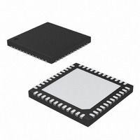
IC I2C GAMMA/VCOM BUFF 48-TQFN
Manufacturer
Maxim Integrated Products
Datasheet
1.DS3510TTR.pdf
(17 pages)
Specifications of DS3510T+T&R
Applications
TFT-LCD Panels: Gamma Buffer, VCOM Driver
Output Type
Rail-to-Rail
Number Of Circuits
10
Current - Supply
6.7mA
Current - Output / Channel
4mA
Voltage - Supply, Single/dual (±)
9 V ~ 15 V
Mounting Type
Surface Mount
Package / Case
48-TQFN Exposed Pad
Lead Free Status / RoHS Status
Lead free / RoHS Compliant
Byte write: A byte write consists of 8 bits of information
transferred from the master to the slave (most signifi-
cant bit first) plus a 1-bit acknowledgment from the
slave to the master. The 8 bits transmitted by the mas-
ter are done according to the bit write definition and the
acknowledgment is read using the bit read definition.
Byte read: A byte read is an 8-bit information transfer
from the slave to the master plus a 1-bit ACK or NACK
from the master to the slave. The 8 bits of information
that are transferred (most significant bit first) from the
slave to the master are read by the master using the bit
read definition above, and the master transmits an ACK
using the bit write definition to receive additional data
bytes. The master must NACK the last byte read to ter-
minate communication so the slave will return control of
SDA to the master.
Slave Address Byte: Each slave on the I
responds to a slave address byte sent immediately fol-
lowing a start condition. The slave address byte con-
tains the slave address in the most significant 7 bits
and the R/W bit in the least significant bit.
The DS3510’s slave address is determined by the state
of the A0 address pin as shown in Figure 5. An address
pin connected to GND results in a 0 in the correspond-
ing bit position in the slave address. Conversely, an
address pin connected to V
responding bit position.
When the R/W bit is 0 (such as in C0h), the master is
indicating it will write data to the slave. If R/W is set to a
1, (C1h in this case), the master is indicating it wants to
read from the slave.
If an incorrect (non-matching) slave address is written,
the DS3510 will assume the master is communicating
with another I
until the next start condition is sent.
Memory address: During an I
DS3510, the master must transmit a memory address to
identify the memory location where the slave is to store
the data. The memory address is always the second
byte transmitted during a write operation following the
slave address byte.
I
2
2
C device and ignore the communication
C Gamma and V
______________________________________________________________________________________
CC
2
results in a 1 in the cor-
C write operation to the
2
C bus
COM
Writing a single byte to a slave: The master must gen-
erate a START condition, write the slave address byte
(R/W = 0), write the memory address, write the byte of
data, and generate a STOP condition. Remember the
master must read the slave’s acknowledgment during
all byte write operations.
When writing to the DS3510 (and if LD = 1), the DAC will
adjust to the new setting once it has acknowledged the
new data that is being written, and the EEPROM (used to
make the setting nonvolatile) will be written following the
STOP condition at the end of the write command.
Writing multiple bytes to a slave: To write multiple
bytes to a slave in one transaction, the master gener-
ates a START condition, writes the slave address byte
(R/W = 0), writes the memory address, writes up to 8
data bytes, and generates a STOP condition. The
DS3510 is capable of writing 1 to 8 bytes (1 page or
row) in a single write transaction. This is internally con-
trolled by an address counter that allows data to be
written to consecutive addresses without transmitting a
memory address before each data byte is sent. The
address counter limits the write to one 8-byte page
(one row of the memory map). The first page begins at
address 00h and subsequent pages begin at multiples
of 8 (08h, 10h, 18h, etc). Attempts to write to additional
pages of memory without sending a STOP condition
between pages results in the address counter wrap-
ping around to the beginning of the present row. To
prevent address wrapping from occurring, the master
must send a STOP condition at the end of the page,
then wait for the bus-free or EEPROM-write time to
elapse. Then the master can generate a new START
condition and write the slave address byte (R/W = 0)
and the first memory address of the next memory row
before continuing to write data.
Acknowledge polling: Any time a EEPROM byte is
written, the DS3510 requires the EEPROM write time
(t
the byte to EEPROM. During the EEPROM write time,
the device will not acknowledge its slave address
because it is busy. It is possible to take advantage of
this phenomenon by repeatedly addressing the
DS3510, which allows communication to continue as
soon as the DS3510 is ready. The alternative to
acknowledge polling is to wait for a maximum period of
t
W
W
to elapse before attempting to access the device.
) after the STOP condition to write the contents of
Buffer with EEPROM
I
2
C Communication
15


