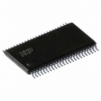
SC28L201A1DGG,112 NXP Semiconductors, SC28L201A1DGG,112 Datasheet - Page 52

SC28L201A1DGG,112
Manufacturer Part Number
SC28L201A1DGG,112
Description
IC UART W/FIFO 48-TSSOP
Manufacturer
NXP Semiconductors
Series
IMPACTr
Datasheet
1.SC28L201A1DGG118.pdf
(110 pages)
Specifications of SC28L201A1DGG,112
Features
False-start Bit Detection
Number Of Channels
2, DUART
Fifo's
256 Byte
Voltage - Supply
3.3V, 5V
With Parallel Port
Yes
With Auto Flow Control
Yes
With False Start Bit Detection
Yes
With Modem Control
Yes
With Cmos
Yes
Mounting Type
Surface Mount
Package / Case
48-TSSOP
Lead Free Status / RoHS Status
Lead free / RoHS Compliant
Other names
568-3293-5
935277824112
SC28L201A1DGG
935277824112
SC28L201A1DGG
Philips Semiconductors
9397 750 13138
Product data sheet
Table 23:
Bit
4:0
Symbol
CRx - Command Register Extension (address 0x12) bit description
Description
Command Register codes
The encoded value of this field can be used to specify a single command as
follows:
0 0000: no command
0 0001: reserved
0 0010: Reset receiver. Immediately resets the receiver as if hardware
reset had been applied. The receiver is reset and the FIFO pointer is reset
to the first location effectively discarding all unread characters in the FIFO.
0 0011: Reset transmitter. Immediately resets the transmitter as if a
hardware reset had been applied. The transmitter is reset and the FIFO
pointer is reset to the first location effectively discarding all un-transmitted
characters in the FIFO.
0 0100: Reset error status. Clears the received break, parity error, framing
error, and overrun error bits in the Status Register (SR[7:4]). It is used in
either character or block mode. In block mode it would normally be used
after the block is read.
0 0101: Reset break change interrupt. Causes the break detect change bit
in the Interrupt Status Register (ISR[2]) to be cleared to zero.
0 0110: Start break. Forces the TXD output LOW (spacing). If the
transmitter is empty, the start of the break condition will be delayed up to
two bit times. If the transmitter is active and the TxFIFO is empty then the
break begins when transmission of the current character is completed. If
there are characters in the TxFIFO, the start of break is delayed until all
characters presently in the TxFIFO and any subsequent characters loaded
have been transmitted. (Tx Idle must be true before break begins). The
transmitter must be enabled to start a break.
0 0111: Stop break. The TXD line will go HIGH (marking) within two bit
times. TXD will remain HIGH for one bit time before the next character is
transmitted.
0 1000: Assert RTSN. Causes the RTSN output to be asserted (LOW).
0 1001: Negate RTSN. Causes the RTSN output to be negated (HIGH).
Remark: The two commands above actually reset and set, respectively,
the I/O0B (Channel A) pin associated with the OPR register. (See
8.6.10 “Set the Output Port Bits OPR A and OPR B (SOPR A and
SOPR B)”
(ROPR A, ROPR
0 1010: Set C/T Receiver time-out mode on.
0 1011: Set MR Pointer to 0.
0 1100: Set C/T Receiver time-out mode off.
0 1101: Block error status accumulation on FIFO entry. Allows the
‘received break’, ‘framing error’, and ‘parity error’ bits to be set as the
received character is loaded to the RxFIFO (normally these bits are set on
reading of the data from the RxFIFO). Setting this mode can give
information about error data up to 256 bytes earlier than the normal mode.
However, it clouds the ability to know precisely which byte(s) are in error.
0 1110: Power-down mode on.
0 1111: Disable Power-down mode.
Rev. 01 — 31 October 2005
and
Section 8.6.11 “Reset Output Port bits OPR A and OPR B
3.3 V, 5 V UART, 3.125 Mbit/s, with 256-byte FIFO
B)”).
© Koninklijke Philips Electronics N.V. 2005. All rights reserved.
SC28L201
…continued
Section
52 of 110


