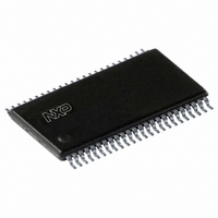
SC28L201A1DGG,112 NXP Semiconductors, SC28L201A1DGG,112 Datasheet - Page 42

SC28L201A1DGG,112
Manufacturer Part Number
SC28L201A1DGG,112
Description
IC UART W/FIFO 48-TSSOP
Manufacturer
NXP Semiconductors
Series
IMPACTr
Datasheet
1.SC28L201A1DGG118.pdf
(110 pages)
Specifications of SC28L201A1DGG,112
Features
False-start Bit Detection
Number Of Channels
2, DUART
Fifo's
256 Byte
Voltage - Supply
3.3V, 5V
With Parallel Port
Yes
With Auto Flow Control
Yes
With False Start Bit Detection
Yes
With Modem Control
Yes
With Cmos
Yes
Mounting Type
Surface Mount
Package / Case
48-TSSOP
Lead Free Status / RoHS Status
Lead free / RoHS Compliant
Other names
568-3293-5
935277824112
SC28L201A1DGG
935277824112
SC28L201A1DGG
Philips Semiconductors
9397 750 13138
Product data sheet
8.2.1 Mode Register 0 (MR0)
MR0 can be accessed directly at H’20’ and 0x20 in the Extended section of the address
map, or by means of the ‘MR Pointers’ at the 0x00 used by legacy code.
Table 12:
[1]
[2]
Bit
7
6
5:4
3
2
1
0
This bit control is duplicated at WCXER[7:6], the Watchdog, Character, Address and X Enable Register.
These bits are used to select one of the six baud rate groups. Combinations of MR0[2:0] other than those
shown below should not be used.
a) Normal Mode: MR0[2:0] = 000
b) Extended Mode I: MR0[2:0] = 001
c) Extended Mode II: MR0[2:0] = 100
Symbol
MR0[7]
MR0[6]
MR0[6] and
MR1[6]
MR0[5:4]
MR0[3]
MR0[2]
MR0[1]
MR0[0]
MR0 - Mode Register 0 (address 0x20) bit description
[1]
[2]
[2]
[2]
Rev. 01 — 31 October 2005
Description
Rx Watchdog. Fixed length watchdog timer.
This bit controls the receiver watchdog timer. 0 = disable, 1 = enable.
When enabled, the watchdog timer will generate a receiver interrupt if the
receiver FIFO has not been accessed within 64 bit times of the receiver
1 clock. This is used to alert the control processor that data is in the
RxFIFO that has not been read. This situation may occur when the byte
count of the last part of a message is not large enough to generate an
interrupt.
RxINT[2]. Bit 2 of receiver FIFO interrupt level. This bit along with Bit 6 of
MR1 sets the fill level of the 8 byte FIFO that generates the receiver
interrupt.
Note that this control is split between MR0 and MR1. This is for backward
compatibility to the SC2692 and SCC2681.
For the receiver, these bits control the number of FIFO positions filled
when the receiver will attempt to interrupt. After the reset the receiver
FIFO is empty. The default setting of these bits cause the receiver to
attempt to interrupt when it has one or more bytes in it. See
Table
TxINT[1:0]. Transmitter interrupt fill level.
For the transmitter, these bits control the number of FIFO positions empty
when the receiver will attempt to interrupt. After the reset the transmit
FIFO has 8 bytes empty. It will then attempt to interrupt as soon as the
transmitter is enabled. The default setting of the MR0 bits (00) condition
the transmitter to attempt to interrupt only when it is completely empty. As
soon as one byte is loaded, it is no longer empty and hence will withdraw
its interrupt request. See
FIFO size. Selects between 8-byte or 256-byte FIFO structure.
Baud rate extended II. (Legacy baud rate group selection.)
reserved; set to 0. (Legacy baud rate group selection.)
Baud rate extended I. (Legacy baud rate group selection.)
0 = disable
1 = enable
0 = 8 bytes
1 = 256 bytes
0 = Normal mode
1 = Extended Mode II
0 = Normal mode
1 = Extended Mode I
14.
3.3 V, 5 V UART, 3.125 Mbit/s, with 256-byte FIFO
Table 15
and
Table
© Koninklijke Philips Electronics N.V. 2005. All rights reserved.
16.
SC28L201
Table 13
42 of 110
and


