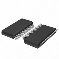
SC28L201A1DGG,118 NXP Semiconductors, SC28L201A1DGG,118 Datasheet - Page 21

SC28L201A1DGG,118
Manufacturer Part Number
SC28L201A1DGG,118
Description
IC UART W/FIFO 48-TSSOP
Manufacturer
NXP Semiconductors
Series
IMPACTr
Datasheet
1.SC28L201A1DGG118.pdf
(110 pages)
Specifications of SC28L201A1DGG,118
Features
False-start Bit Detection
Number Of Channels
2, DUART
Fifo's
256 Byte
Voltage - Supply
3.3V, 5V
With Parallel Port
Yes
With Auto Flow Control
Yes
With False Start Bit Detection
Yes
With Modem Control
Yes
With Cmos
Yes
Mounting Type
Surface Mount
Package / Case
48-TSSOP
Lead Free Status / RoHS Status
Lead free / RoHS Compliant
Other names
935277824118
SC28L201A1DGG-T
SC28L201A1DGG-T
SC28L201A1DGG-T
SC28L201A1DGG-T
Philips Semiconductors
9397 750 13138
Product data sheet
7.4.7.1 1x and 16x modes, receiver
7.4.7.2 Receiver
The receiver operates in one of two modes: 1 and 16 . Of the two, the 16 is by far more
robust and the preferred mode. Although the 1 mode may allow a faster data rate, it
does not provide for the alignment of the receiver 1 data clock to that of the transmitter.
This strongly implies that the 1 clock of the remote transmitter is available to the receiver;
the two devices are physically close to each other.
The 16 mode operates the receiver logic at a rate 16 times faster than the 1 data rate.
This allows for validation of the start bit length, the validation of level changes at the
receiver serial data input (RXD), and the validation of the stop bit length. Of most
importance in the 16 mode is the ability of the receiver logic to align the phase of the
internally generated receiver 1 data clock to that of the received start bit of the remote
transmitter. This occurs with an accuracy of less than
The receiver of the SC28L201 is conditioned to receive data when enabled through the
Command Register. The receiver looks for a HIGH-to-LOW (mark-to-space) transition of
the start bit on the RXD input pin. If a transition is detected, the state of the RXD pin is
sampled each 16 clock for 7
of the bit time clock (1 clock mode). If RXD is sampled HIGH, (that is the start bit was
LOW less than
another valid start bit begins immediately. If RXD is still LOW, a valid start bit is assumed
and the receiver then continues to sample the input at one-bit time intervals at the
theoretical center of the bit. When the proper number of data bits and parity bit (if used)
have been assembled, and one half-stop bit has been detected the receiver loads the byte
to the FIFO. The least significant bit is received first. The data is then transferred to the
Receive FIFO and the ISR RxRDY bit in the SR is set to ‘1’. This condition can be
programmed to generate an interrupt at IRQN or I/O[4]B. If the character length is less
than 8 bits, the most significant unused bits in the RxFIFO are set to zero.
After the stop bit is detected, the receiver will immediately look for the next start bit.
However, if a non-zero character was received with the stop bit at a zero level (framing
error) and RXD remains LOW for at least another
sampled, then the receiver operates as if a new start bit had been detected. It then
continues assembling the next character.
The error conditions of parity error, framing error, and overrun error (if any) are written to
the SR at the received character boundary. This is just before the RxRDY status bit is set.
A break condition is detected when RXD is LOW for the entire character including the
parity bit, if used, and stop bit. When a break is found a character consisting of all zeros
will be loaded into the RxFIFO, the received break bit in the SR and the change of break
bit in the ISR are set to 1 and the receiver ready is set in the SR. The RXD input must
return to HIGH for two (2) clock edges of the RxC1x clock for the receiver to recognize
the end of the break condition. At the end of the break condition the search for the next
start bit begins.
Two edges of the RxC1x clock will usually require a HIGH time of one RxC1x clock period
or 3 RxC1x edges since the clock of the controller is usually not synchronous to nor in
phase with the RxC1x clock.
7
16
-bit to
Rev. 01 — 31 October 2005
1
2
-bit time) the start bit is judged invalid and the search for
1
2
clock periods (16 clock mode) or at the next rising edge
3.3 V, 5 V UART, 3.125 Mbit/s, with 256-byte FIFO
1
2
-bit time after the stop bit was
1
16
-bit time.
© Koninklijke Philips Electronics N.V. 2005. All rights reserved.
SC28L201
21 of 110


