SC28L92A1B,557 NXP Semiconductors, SC28L92A1B,557 Datasheet - Page 73
SC28L92A1B,557
Manufacturer Part Number
SC28L92A1B,557
Description
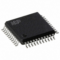
IC UART DUAL W/FIFO 44-PQFP
Manufacturer
NXP Semiconductors
Series
IMPACTr
Type
Dual UARTr
Datasheet
1.SC28L92A1B557.pdf
(73 pages)
Specifications of SC28L92A1B,557
Number Of Channels
2, DUART
Package / Case
44-MQFP, 44-PQFP
Features
False-start Bit Detection
Fifo's
16 Byte
Voltage - Supply
3.3V, 5V
With Auto Flow Control
Yes
With False Start Bit Detection
Yes
With Modem Control
Yes
With Cmos
Yes
Mounting Type
Surface Mount
Data Rate
0.2304 MBd
Supply Voltage (max)
3.63 V or 5.5 V
Supply Voltage (min)
2.97 V or 4.5 V
Supply Current
25 mA
Maximum Operating Temperature
+ 85 C
Minimum Operating Temperature
- 40 C
Mounting Style
SMD/SMT
Operating Supply Voltage
3.3 V or 5 V
Lead Free Status / RoHS Status
Lead free / RoHS Compliant
Lead Free Status / RoHS Status
Lead free / RoHS Compliant, Lead free / RoHS Compliant
Other names
568-1211
935263294557
SC28L92A1B
935263294557
SC28L92A1B
Available stocks
Company
Part Number
Manufacturer
Quantity
Price
Company:

Part Number:
SC28L92A1B,557
Manufacturer:
NXP Semiconductors
Quantity:
10 000


NXP Semiconductors
19. Contents
1
2
3
4
5
5.1
5.2
6
6.1
6.1.1
6.1.2
6.1.3
6.1.4
6.1.5
6.2
6.2.1
6.2.2
6.2.3
6.2.4
6.2.5
6.2.6
6.2.7
6.2.8
6.2.9
6.2.10
6.3
6.3.1
6.3.2
6.3.3
6.3.4
6.3.5
6.3.6
6.3.7
6.3.8
6.3.9
6.3.10
7
7.1
7.2
7.3
7.3.1
7.3.1.1
7.3.1.2
7.3.1.3
7.3.1.4
7.3.1.5
7.3.1.6
General description . . . . . . . . . . . . . . . . . . . . . . 1
Features . . . . . . . . . . . . . . . . . . . . . . . . . . . . . . . 2
Ordering information . . . . . . . . . . . . . . . . . . . . . 3
Block diagram . . . . . . . . . . . . . . . . . . . . . . . . . . 4
Pinning information . . . . . . . . . . . . . . . . . . . . . . 6
Functional description . . . . . . . . . . . . . . . . . . 13
Programming . . . . . . . . . . . . . . . . . . . . . . . . . . 22
Pinning . . . . . . . . . . . . . . . . . . . . . . . . . . . . . . . 6
Pin description . . . . . . . . . . . . . . . . . . . . . . . . . 9
Block diagram . . . . . . . . . . . . . . . . . . . . . . . . . 13
Data bus buffer . . . . . . . . . . . . . . . . . . . . . . . . 13
Operation control . . . . . . . . . . . . . . . . . . . . . . 13
Interrupt control . . . . . . . . . . . . . . . . . . . . . . . 13
FIFO configuration . . . . . . . . . . . . . . . . . . . . . 14
68xxx mode . . . . . . . . . . . . . . . . . . . . . . . . . . 14
Timing circuits. . . . . . . . . . . . . . . . . . . . . . . . . 14
Crystal clock . . . . . . . . . . . . . . . . . . . . . . . . . . 14
Baud rate generator . . . . . . . . . . . . . . . . . . . . 15
Counter/timer . . . . . . . . . . . . . . . . . . . . . . . . . 15
Timer mode. . . . . . . . . . . . . . . . . . . . . . . . . . . 15
Counter mode . . . . . . . . . . . . . . . . . . . . . . . . . 16
Time-out mode . . . . . . . . . . . . . . . . . . . . . . . . 16
Time-out mode caution . . . . . . . . . . . . . . . . . . 17
Communications channels A and B . . . . . . . . 17
Input port . . . . . . . . . . . . . . . . . . . . . . . . . . . . 17
Output port . . . . . . . . . . . . . . . . . . . . . . . . . . . 18
Operation . . . . . . . . . . . . . . . . . . . . . . . . . . . . 18
Transmitter . . . . . . . . . . . . . . . . . . . . . . . . . . . 18
Receiver . . . . . . . . . . . . . . . . . . . . . . . . . . . . . 19
Transmitter reset and disable . . . . . . . . . . . . . 19
Receiver FIFO . . . . . . . . . . . . . . . . . . . . . . . . 20
Receiver status bits . . . . . . . . . . . . . . . . . . . . 20
Receiver reset and disable . . . . . . . . . . . . . . . 20
Watchdog . . . . . . . . . . . . . . . . . . . . . . . . . . . . 21
Receiver time-out mode . . . . . . . . . . . . . . . . . 21
Time-out mode caution . . . . . . . . . . . . . . . . . . 22
Multi-drop mode (9-bit or wake-up). . . . . . . . . 22
Register overview . . . . . . . . . . . . . . . . . . . . . . 22
Condensed register bit formats. . . . . . . . . . . . 24
Register descriptions . . . . . . . . . . . . . . . . . . . 26
Mode registers . . . . . . . . . . . . . . . . . . . . . . . . 26
Mode Register 0 channel A (MR0A) . . . . . . . . 26
Mode Register 1 channel A (MR1A) . . . . . . . . 28
Mode Register 2 channel A (MR2A) . . . . . . . . 29
Mode Register 0 channel B (MR0B) . . . . . . . . 32
Mode Register 1 channel B (MR1B) . . . . . . . . 32
Mode Register 2 channel B (MR2B) . . . . . . . . 32
3.3 V/5.0 V Dual Universal Asynchronous Receiver/Transmitter
7.3.2
7.3.2.1
7.3.2.2
7.3.3
7.3.3.1
7.3.3.2
7.3.4
7.3.4.1
7.3.4.2
7.3.5
7.3.6
7.3.7
7.3.8
7.3.9
7.3.10
7.3.11
7.3.12
7.3.13
7.3.14
7.4
7.5
8
9
10
11
12
13
14
14.1
14.2
14.3
14.4
15
16
17
17.1
17.2
17.3
17.4
18
19
Please be aware that important notices concerning this document and the product(s)
described herein, have been included in section ‘Legal information’.
© NXP B.V. 2007.
For more information, please visit: http://www.nxp.com
For sales office addresses, please send an email to: salesaddresses@nxp.com
Limiting values . . . . . . . . . . . . . . . . . . . . . . . . 50
Static characteristics . . . . . . . . . . . . . . . . . . . 51
Dynamic characteristics . . . . . . . . . . . . . . . . . 54
Timing diagrams . . . . . . . . . . . . . . . . . . . . . . . 58
Test information. . . . . . . . . . . . . . . . . . . . . . . . 64
Package outline . . . . . . . . . . . . . . . . . . . . . . . . 65
Soldering . . . . . . . . . . . . . . . . . . . . . . . . . . . . . 68
Abbreviations . . . . . . . . . . . . . . . . . . . . . . . . . 70
Revision history . . . . . . . . . . . . . . . . . . . . . . . 71
Legal information . . . . . . . . . . . . . . . . . . . . . . 72
Contact information . . . . . . . . . . . . . . . . . . . . 72
Contents. . . . . . . . . . . . . . . . . . . . . . . . . . . . . . 73
Clock select registers . . . . . . . . . . . . . . . . . . . 33
Clock Select Register channel A (CSRA). . . . 33
Clock Select Register channel B (CSRB). . . . 34
Command registers . . . . . . . . . . . . . . . . . . . . 35
Command Register channel A (CRA) . . . . . . 35
Command Register channel B (CRB) . . . . . . 36
Status registers . . . . . . . . . . . . . . . . . . . . . . . 37
Status Register channel A (SRA). . . . . . . . . . 37
Status Register channel B (SRB). . . . . . . . . . 39
Output Configuration Control Register
(OPCR) . . . . . . . . . . . . . . . . . . . . . . . . . . . . . 39
Set Output Port bits Register (SOPR) . . . . . . 41
Reset Output Port bits Register (ROPR) . . . . 42
Output Port Register (OPR) . . . . . . . . . . . . . . 43
Auxiliary Control Register (ACR) . . . . . . . . . . 44
Input Port Change Register (IPCR) . . . . . . . . 45
Interrupt Status Register (ISR). . . . . . . . . . . . 45
Interrupt Mask Register (IMR) . . . . . . . . . . . . 47
Interrupt Vector Register (IVR; 68xxx mode)
or General Purpose register
(GP; 80xxx mode) . . . . . . . . . . . . . . . . . . . . . 48
Counter/timer registers. . . . . . . . . . . . . . . . . . 48
Output port notes . . . . . . . . . . . . . . . . . . . . . . 49
The CTS, RTS, CTS enable Tx signals . . . . . 49
Introduction to soldering. . . . . . . . . . . . . . . . . 68
Wave and reflow soldering . . . . . . . . . . . . . . . 68
Wave soldering. . . . . . . . . . . . . . . . . . . . . . . . 68
Reflow soldering. . . . . . . . . . . . . . . . . . . . . . . 69
Data sheet status . . . . . . . . . . . . . . . . . . . . . . 72
Definitions . . . . . . . . . . . . . . . . . . . . . . . . . . . 72
Disclaimers. . . . . . . . . . . . . . . . . . . . . . . . . . . 72
Trademarks . . . . . . . . . . . . . . . . . . . . . . . . . . 72
Date of release: 19 December 2007
Document identifier: SC28L92_7
SC28L92
All rights reserved.
Related parts for SC28L92A1B,557
Image
Part Number
Description
Manufacturer
Datasheet
Request
R

Part Number:
Description:
NXP Semiconductors designed the LPC2420/2460 microcontroller around a 16-bit/32-bitARM7TDMI-S CPU core with real-time debug interfaces that include both JTAG andembedded trace
Manufacturer:
NXP Semiconductors
Datasheet:

Part Number:
Description:
NXP Semiconductors designed the LPC2458 microcontroller around a 16-bit/32-bitARM7TDMI-S CPU core with real-time debug interfaces that include both JTAG andembedded trace
Manufacturer:
NXP Semiconductors
Datasheet:
Part Number:
Description:
NXP Semiconductors designed the LPC2468 microcontroller around a 16-bit/32-bitARM7TDMI-S CPU core with real-time debug interfaces that include both JTAG andembedded trace
Manufacturer:
NXP Semiconductors
Datasheet:
Part Number:
Description:
NXP Semiconductors designed the LPC2470 microcontroller, powered by theARM7TDMI-S core, to be a highly integrated microcontroller for a wide range ofapplications that require advanced communications and high quality graphic displays
Manufacturer:
NXP Semiconductors
Datasheet:
Part Number:
Description:
NXP Semiconductors designed the LPC2478 microcontroller, powered by theARM7TDMI-S core, to be a highly integrated microcontroller for a wide range ofapplications that require advanced communications and high quality graphic displays
Manufacturer:
NXP Semiconductors
Datasheet:
Part Number:
Description:
The Philips Semiconductors XA (eXtended Architecture) family of 16-bit single-chip microcontrollers is powerful enough to easily handle the requirements of high performance embedded applications, yet inexpensive enough to compete in the market for hi
Manufacturer:
NXP Semiconductors
Datasheet:
Part Number:
Description:
The XA-S3 device is a member of Philips Semiconductors? XA(eXtended Architecture) family of high performance 16-bitsingle-chip microcontrollers
Manufacturer:
NXP Semiconductors
Datasheet:

Part Number:
Description:
The NXP BlueStreak LH75401/LH75411 family consists of two low-cost 16/32-bit System-on-Chip (SoC) devices
Manufacturer:
NXP Semiconductors
Datasheet:
Part Number:
Description:
The NXP LPC3130/3131 combine an 180 MHz ARM926EJ-S CPU core, high-speed USB2
Manufacturer:
NXP Semiconductors
Datasheet:
Part Number:
Description:
The NXP LPC3141 combine a 270 MHz ARM926EJ-S CPU core, High-speed USB 2
Manufacturer:
NXP Semiconductors
Part Number:
Description:
The NXP LPC3143 combine a 270 MHz ARM926EJ-S CPU core, High-speed USB 2
Manufacturer:
NXP Semiconductors

Part Number:
Description:
The NXP LPC3152 combines an 180 MHz ARM926EJ-S CPU core, High-speed USB 2
Manufacturer:
NXP Semiconductors
Part Number:
Description:
The NXP LPC3154 combines an 180 MHz ARM926EJ-S CPU core, High-speed USB 2
Manufacturer:
NXP Semiconductors

Part Number:
Description:
Standard level N-channel enhancement mode Field-Effect Transistor (FET) in a plastic package using NXP High-Performance Automotive (HPA) TrenchMOS technology
Manufacturer:
NXP Semiconductors
Datasheet: