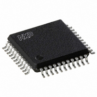
SC28L92A1B,557 NXP Semiconductors, SC28L92A1B,557 Datasheet - Page 12

SC28L92A1B,557
Manufacturer Part Number
SC28L92A1B,557
Description
IC UART DUAL W/FIFO 44-PQFP
Manufacturer
NXP Semiconductors
Series
IMPACTr
Type
Dual UARTr
Datasheet
1.SC28L92A1B557.pdf
(73 pages)
Specifications of SC28L92A1B,557
Number Of Channels
2, DUART
Package / Case
44-MQFP, 44-PQFP
Features
False-start Bit Detection
Fifo's
16 Byte
Voltage - Supply
3.3V, 5V
With Auto Flow Control
Yes
With False Start Bit Detection
Yes
With Modem Control
Yes
With Cmos
Yes
Mounting Type
Surface Mount
Data Rate
0.2304 MBd
Supply Voltage (max)
3.63 V or 5.5 V
Supply Voltage (min)
2.97 V or 4.5 V
Supply Current
25 mA
Maximum Operating Temperature
+ 85 C
Minimum Operating Temperature
- 40 C
Mounting Style
SMD/SMT
Operating Supply Voltage
3.3 V or 5 V
Lead Free Status / RoHS Status
Lead free / RoHS Compliant
Lead Free Status / RoHS Status
Lead free / RoHS Compliant, Lead free / RoHS Compliant
Other names
568-1211
935263294557
SC28L92A1B
935263294557
SC28L92A1B
Available stocks
Company
Part Number
Manufacturer
Quantity
Price
Company:
Part Number:
SC28L92A1B,557
Manufacturer:
NXP Semiconductors
Quantity:
10 000
NXP Semiconductors
Table 3.
SC28L92_7
Product data sheet
Symbol
INTRN
X1/CLK
X2
RxDA
RxDB
TxDA
TxDB
OP0
OP1
OP2
OP3
OP4
OP5
OP6
OP7
IP0
IP1
IP2
Pin
PLCC44 QFP44 HVQFN48
24
36
37
35
11
33
13
32
14
31
15
30
16
29
17
8
5
40
Pin description for 68xxx bus interface (Motorola)
18
30
31
29
5
28
6
27
7
26
8
25
9
24
10
2
43
34
19
32
33
31
5
30
8
29
9
28
10
27
11
26
12
2
47
38
Type
O
I
O
I
I
O
O
O
O
O
O
O
O
O
O
I
I
I
Rev. 07 — 19 December 2007
3.3 V/5.0 V Dual Universal Asynchronous Receiver/Transmitter
Description
Interrupt request: Active LOW, open-drain, output which signals the
CPU that one or more of the eight maskable interrupting conditions
are true. This pin requires a pull-up.
Crystal 1: Crystal or external clock input. A crystal or clock of the
specified limits must be supplied at all times. When a crystal is used, a
capacitor must be connected from this pin to ground (see
Crystal 2: Connection for other side of the crystal. When a crystal is
used, a capacitor must be connected from this pin to ground (see
Figure
be left open.
Channel A receiver serial data input: The least significant bit is
received first. See note on drive levels at block diagram
Channel B receiver serial data input: The least significant bit is
received first. See note on drive levels at block diagram
Channel A transmitter serial data output: The least significant bit is
transmitted first. This output is held in the ‘mark condition when the
transmitter is disabled, idle or when operating in local loopback mode.
See note on drive levels at block diagram
Channel B transmitter serial data output: The least significant bit is
transmitted first. This output is held in the Mark condition when the
transmitter is disabled, idle, or when operating in local loopback mode.
See note on drive levels at block diagram
Output 0: General purpose output or channel A request to send
(RTSAN, active LOW). Can be deactivated automatically on receive or
transmit.
Output 1: General purpose output or channel B request to send
(RTSBN, active LOW). Can be deactivated automatically on receive or
transmit.
Output 2: General purpose output, or channel A transmitter 1 or 16
clock output, or channel A receiver 1 clock output.
Output 3: General purpose output or open-drain, active LOW
counter/timer output or channel B transmitter 1 clock output, or
channel B receiver 1 clock output.
Output 4: General purpose output or channel A open-drain, active
LOW, RxA interrupt ISR [1] output.
Output 5: General purpose output or channel B open-drain, active
LOW, RxB interrupt ISR[5] output.
Output 6: General purpose output or channel A open-drain, active
LOW, TxA interrupt ISR[0] output.
Output 7: General purpose output, or channel B open-drain, active
LOW, TxB interrupt ISR[4] output.
Input 0: General purpose input or channel A clear to send active LOW
input (CTSAN).
Input 1: General purpose input or channel B clear to send active LOW
input (CTSBN).
Input 2: General purpose input or counter/timer external clock input.
17). If X1/CLK is driven from an external source, this pin must
…continued
(Figure
(Figure
2).
2).
SC28L92
© NXP B.V. 2007. All rights reserved.
(Figure
(Figure
Figure
12 of 73
2).
2).
17).


