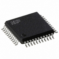
SC28L92A1B,557 NXP Semiconductors, SC28L92A1B,557 Datasheet - Page 39

SC28L92A1B,557
Manufacturer Part Number
SC28L92A1B,557
Description
IC UART DUAL W/FIFO 44-PQFP
Manufacturer
NXP Semiconductors
Series
IMPACTr
Type
Dual UARTr
Datasheet
1.SC28L92A1B557.pdf
(73 pages)
Specifications of SC28L92A1B,557
Number Of Channels
2, DUART
Package / Case
44-MQFP, 44-PQFP
Features
False-start Bit Detection
Fifo's
16 Byte
Voltage - Supply
3.3V, 5V
With Auto Flow Control
Yes
With False Start Bit Detection
Yes
With Modem Control
Yes
With Cmos
Yes
Mounting Type
Surface Mount
Data Rate
0.2304 MBd
Supply Voltage (max)
3.63 V or 5.5 V
Supply Voltage (min)
2.97 V or 4.5 V
Supply Current
25 mA
Maximum Operating Temperature
+ 85 C
Minimum Operating Temperature
- 40 C
Mounting Style
SMD/SMT
Operating Supply Voltage
3.3 V or 5 V
Lead Free Status / RoHS Status
Lead free / RoHS Compliant
Lead Free Status / RoHS Status
Lead free / RoHS Compliant, Lead free / RoHS Compliant
Other names
568-1211
935263294557
SC28L92A1B
935263294557
SC28L92A1B
Available stocks
Company
Part Number
Manufacturer
Quantity
Price
Company:
Part Number:
SC28L92A1B,557
Manufacturer:
NXP Semiconductors
Quantity:
10 000
NXP Semiconductors
SC28L92_7
Product data sheet
7.3.4.2 Status Register channel B (SRB)
7.3.5 Output Configuration Control Register (OPCR)
Table 43.
[1]
The bit definitions for this register are identical to the bit definitions for SRA, except that all
status applies to the channel B receiver and transmitter and the corresponding inputs and
outputs.
This register controls the signal presented by the OP[7:2] pins. The signal presented by
the OP[1:0] pins is controlled by the Rx, Tx, and the command register. The default
condition of the OP pins is to drive the complement of the data in the OPR[7:0] register.
When OP[7:2] pins drive DMA or interrupt type signals, they switch to open-drain
configuration. Otherwise, they drive strong logic 0 or logic 1 levels.
Table 44.
Table 45.
Bit
7
6
5
4
configure
received
break
OP7
These status bits are appended to the corresponding data character in the receive FIFO. A read of the
status provides these bits [7:5] from the top of the FIFO together with bits [4:0]. These bits are cleared by a
reset error status command. In character mode they are discarded when the corresponding data character
is read from the FIFO. In block error mode, the error-reset command (command 0x4 or receiver reset) must
used to clear block error conditions.
7
7
[1]
Symbol
-
-
-
-
SRB - Status register channel B (address 0x9) bit allocation
OPCR - Output configuration control register (address 0xD) bit allocation
OPCR - Output configuration control register (address 0xD) bit description
configure
framing
error
OP6
6
6
[1]
Description
OP7 output select
OP6 output select
OP5 output select
OP4 output select
Rev. 07 — 19 December 2007
0 = The complement of OPR[7]
1 = The channel B transmitter interrupt output which is the complement of
ISR[4]. When in this mode OP7 acts as an open-drain output. Note that
this output is not masked by the contents of the IMR.
0 = The complement of OPR[6]
1 = The channel A transmitter interrupt output which is the complement of
ISR[0]. When in this mode OP6 acts as an open-drain output. Note that
this output is not masked by the contents of the IMR.
0 = The complement of OPR[5]
1 = The channel B receiver interrupt output which is the complement of
ISR[5]. When in this mode OP5 acts as an open-drain output. Note that
this output is not masked by the contents of the IMR.
0 = The complement of OPR[4]
1 = The channel A receiver interrupt output which is the complement of
ISR[1]. When in this mode OP4 acts as an open-drain output. Note that
this output is not masked by the contents of the IMR.
3.3 V/5.0 V Dual Universal Asynchronous Receiver/Transmitter
configure
error
parity
OP5
5
5
[1]
overrun
configure
error
4
OP4
4
TxEMTB
3
configure OP3
3
TxRDYB
2
2
RxFULLB
SC28L92
© NXP B.V. 2007. All rights reserved.
1
configure OP2
1
RxRDYB
39 of 73
0
0


