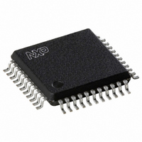
SC28L92A1B,557 NXP Semiconductors, SC28L92A1B,557 Datasheet - Page 19

SC28L92A1B,557
Manufacturer Part Number
SC28L92A1B,557
Description
IC UART DUAL W/FIFO 44-PQFP
Manufacturer
NXP Semiconductors
Series
IMPACTr
Type
Dual UARTr
Datasheet
1.SC28L92A1B557.pdf
(73 pages)
Specifications of SC28L92A1B,557
Number Of Channels
2, DUART
Package / Case
44-MQFP, 44-PQFP
Features
False-start Bit Detection
Fifo's
16 Byte
Voltage - Supply
3.3V, 5V
With Auto Flow Control
Yes
With False Start Bit Detection
Yes
With Modem Control
Yes
With Cmos
Yes
Mounting Type
Surface Mount
Data Rate
0.2304 MBd
Supply Voltage (max)
3.63 V or 5.5 V
Supply Voltage (min)
2.97 V or 4.5 V
Supply Current
25 mA
Maximum Operating Temperature
+ 85 C
Minimum Operating Temperature
- 40 C
Mounting Style
SMD/SMT
Operating Supply Voltage
3.3 V or 5 V
Lead Free Status / RoHS Status
Lead free / RoHS Compliant
Lead Free Status / RoHS Status
Lead free / RoHS Compliant, Lead free / RoHS Compliant
Other names
568-1211
935263294557
SC28L92A1B
935263294557
SC28L92A1B
Available stocks
Company
Part Number
Manufacturer
Quantity
Price
Company:
Part Number:
SC28L92A1B,557
Manufacturer:
NXP Semiconductors
Quantity:
10 000
NXP Semiconductors
SC28L92_7
Product data sheet
6.3.2 Receiver
6.3.3 Transmitter reset and disable
If CTS option is enabled (MR2[4] = 1), the CTS input at IP0 or IP1 must be LOW in order
for the character to be transmitted. The transmitter will check the state of the CTS input at
the beginning of each character transmitted. If it is found to be HIGH, the transmitter will
delay the transmission of any following characters until the CTS has returned to the LOW
state. CTS going HIGH during the serialization of a character will not affect that character.
The transmitter can also control the RTSN outputs, OP0 or OP1 via MR2[5]. When this
mode of operation is set, the meaning of the OP0 or OP1 signals will usually be end of
message. See description of bit MR2[5] in
(address 0x0) bit description”
turn around a transceiver in simplex systems.
The SC28L92 is conditioned to receive data when enabled through the command register.
The receiver looks for a HIGH-to-LOW (mark-to-space) transition of the start bit on the
RxD input pin. If a transition is detected, the state of the RxD pin is sampled each 16
clock for 7 clocks to
clock (1 clock mode). If RxD is sampled HIGH, the start bit is invalid and the search for a
valid start bit begins again. If RxD is still LOW, a valid start bit is assumed and the receiver
continues to sample the input at one bit time intervals at the theoretical center of the bit,
until the proper number of data bits and parity bit (if any) have been assembled, and one
stop bit has been detected. The least significant bit is received first. The data is then
transferred to the receive FIFO and the RxRDY bit in the SR is set to a 1. This condition
can be programmed to generate an interrupt at OP4 or OP5 and INTRN. If the character
length is less than 8 bits, the most significant unused bits in the Rx FIFO are set to zero.
After the stop bit is detected, the receiver will immediately look for the next start bit.
However, if a non-zero character was received without a stop bit (framing error) and RxD
remains LOW for one half of the bit period after the stop bit was sampled, then the
receiver operates as if a new start bit transition had been detected at that point (one-half
bit time after the stop bit was sampled).
The parity error, framing error and overrun error (if any) are strobed into the SR from the
next byte to be read from the Rx FIFO. If a break condition is detected (RxD is LOW for
the entire character including the stop bit), a character consisting of all zeros will be
loaded into the Rx FIFO and the received break bit in the SR is set to 1. The RxD input
must return to HIGH for two (2) clock edges of the X1 crystal clock for the receiver to
recognize the end of the break condition and begin the search for a start bit.
This will usually require a HIGH time of one X1 clock period or 3 X1 edges since the
clock of the controller is not synchronous to the X1 clock.
Note the difference between transmitter disable and reset. A transmitter reset stops
transmitter action immediately, clears the transmitter FIFO and returns the idle state. A
transmitter disable withdraws the transmitter interrupts but allows the transmitter to
continue operation until all bytes in its FIFO and shift register have been transmitted
including the final stop bits. It then returns to its idle state.
1
Rev. 07 — 19 December 2007
2
3.3 V/5.0 V Dual Universal Asynchronous Receiver/Transmitter
clocks (16 clock mode) or at the next rising edge of the bit time
for more detail. This feature may be used to automatically
Table 30 “MR2A - Mode Register 2 channel A
SC28L92
© NXP B.V. 2007. All rights reserved.
19 of 73


