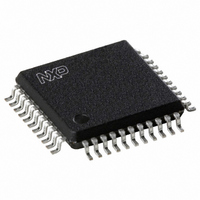
SC28L92A1B,557 NXP Semiconductors, SC28L92A1B,557 Datasheet - Page 44

SC28L92A1B,557
Manufacturer Part Number
SC28L92A1B,557
Description
IC UART DUAL W/FIFO 44-PQFP
Manufacturer
NXP Semiconductors
Series
IMPACTr
Type
Dual UARTr
Datasheet
1.SC28L92A1B557.pdf
(73 pages)
Specifications of SC28L92A1B,557
Number Of Channels
2, DUART
Package / Case
44-MQFP, 44-PQFP
Features
False-start Bit Detection
Fifo's
16 Byte
Voltage - Supply
3.3V, 5V
With Auto Flow Control
Yes
With False Start Bit Detection
Yes
With Modem Control
Yes
With Cmos
Yes
Mounting Type
Surface Mount
Data Rate
0.2304 MBd
Supply Voltage (max)
3.63 V or 5.5 V
Supply Voltage (min)
2.97 V or 4.5 V
Supply Current
25 mA
Maximum Operating Temperature
+ 85 C
Minimum Operating Temperature
- 40 C
Mounting Style
SMD/SMT
Operating Supply Voltage
3.3 V or 5 V
Lead Free Status / RoHS Status
Lead free / RoHS Compliant
Lead Free Status / RoHS Status
Lead free / RoHS Compliant, Lead free / RoHS Compliant
Other names
568-1211
935263294557
SC28L92A1B
935263294557
SC28L92A1B
Available stocks
Company
Part Number
Manufacturer
Quantity
Price
Company:
Part Number:
SC28L92A1B,557
Manufacturer:
NXP Semiconductors
Quantity:
10 000
NXP Semiconductors
Table 52.
SC28L92_7
Product data sheet
BRG set
select
7
ACR - Auxiliary control register (address 0x4) bit allocation
7.3.9 Auxiliary Control Register (ACR)
counter/timer mode and clock source select
6
Table 53.
Table 54.
[1]
Bit
7
6 to 4
3 to 0
ACR[6:4]
000
001
010
011
100
101
110
111
The timer mode generates a square wave.
Symbol
-
-
-
ACR - Auxiliary control register (address 0x4) bit description
ACR[6:4] field definition
5
Mode
counter
counter
counter
counter
timer
timer
timer
timer
Description
Baud rate generator set select.
This bit selects one of two sets of baud rates to be generated by the BRG (see
Table
The selected set of rates is available for use by the channel A and B receivers
and transmitters as described for CSRA in
Baud rate generator characteristics are given in
Counter/timer mode and clock source select.
This field selects the operating mode of the counter/timer and its clock source
as shown in
IP3, IP2, IP1 and IP0 change-of-state interrupt enable.
This field selects which bits of the input port change register (IPCR) cause the
input change bit in the interrupt status register (ISR [7]) to be set. If a bit is in
the enabled state the setting of the corresponding bit in the IPCR will also
result in the setting of ISR [7], which results in the generation of an interrupt
output if IMR [7] = 1. If a bit is in the off state, the setting of that bit in the IPCR
has no effect on ISR [7].
0 = off
1 = enabled
Rev. 07 — 19 December 2007
3.3 V/5.0 V Dual Universal Asynchronous Receiver/Transmitter
35).
4
Table
COS interrupt
[1]
enable IP3
54.
Clock source
external (IP2)
TxCA - 1 clock of channel A transmitter
TxCB - 1 clock of channel B transmitter
crystal or external clock (X1/CLK) divided by 16
external (IP2)
external (IP2) divided by 16
crystal or external clock (X1/CLK)
crystal or external clock (X1/CLK) divided by 16
3
COS interrupt
enable IP2
2
Table 34
Table
COS interrupt
enable IP1
and for CSRB in
36.
1
SC28L92
© NXP B.V. 2007. All rights reserved.
COS interrupt
enable IP0
Table
0
44 of 73
37.


