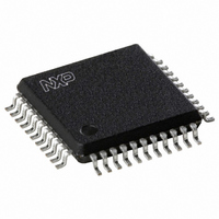
SC28L92A1B,557 NXP Semiconductors, SC28L92A1B,557 Datasheet - Page 11

SC28L92A1B,557
Manufacturer Part Number
SC28L92A1B,557
Description
IC UART DUAL W/FIFO 44-PQFP
Manufacturer
NXP Semiconductors
Series
IMPACTr
Type
Dual UARTr
Datasheet
1.SC28L92A1B557.pdf
(73 pages)
Specifications of SC28L92A1B,557
Number Of Channels
2, DUART
Package / Case
44-MQFP, 44-PQFP
Features
False-start Bit Detection
Fifo's
16 Byte
Voltage - Supply
3.3V, 5V
With Auto Flow Control
Yes
With False Start Bit Detection
Yes
With Modem Control
Yes
With Cmos
Yes
Mounting Type
Surface Mount
Data Rate
0.2304 MBd
Supply Voltage (max)
3.63 V or 5.5 V
Supply Voltage (min)
2.97 V or 4.5 V
Supply Current
25 mA
Maximum Operating Temperature
+ 85 C
Minimum Operating Temperature
- 40 C
Mounting Style
SMD/SMT
Operating Supply Voltage
3.3 V or 5 V
Lead Free Status / RoHS Status
Lead free / RoHS Compliant
Lead Free Status / RoHS Status
Lead free / RoHS Compliant, Lead free / RoHS Compliant
Other names
568-1211
935263294557
SC28L92A1B
935263294557
SC28L92A1B
Available stocks
Company
Part Number
Manufacturer
Quantity
Price
Company:
Part Number:
SC28L92A1B,557
Manufacturer:
NXP Semiconductors
Quantity:
10 000
NXP Semiconductors
Table 2.
[1]
Table 3.
SC28L92_7
Product data sheet
Symbol
GND
n.c.
Symbol
I/M
D0
D1
D2
D3
D4
D5
D6
D7
CEN
R/WN
IACKN
DACKN
A0
A1
A2
A3
RESETN 38
HVQFN48 package die supply ground is connected to both GND pin and exposed center pad. GND pin must be connected to supply
ground for proper device operation. For enhanced thermal, electrical, and board level performance, the exposed pad needs to be
soldered to the board using a corresponding thermal pad on the board and for proper heat conduction through the board, thermal vias
need to be incorporated in the PCB in the thermal pad region.
Pin
PLCC44 QFP44 HVQFN48
22
1, 23, 34 23
Pin
PLCC44 QFP44 HVQFN48
12
28
18
27
19
26
20
25
21
39
9
41
10
2
4
6
7
Pin description for 80xxx bus interface (Intel)
Pin description for 68xxx bus interface (Motorola)
16, 17
11
22
12
21
13
20
14
19
15
33
3
35
4
40
42
44
1
32
18
6, 13, 24, 25,
36, 37, 43
7
23
14
22
15
21
16
20
17
35
3
39
4
44
46
48
1
34
[1]
Type
Pwr
Pwr
Type
I
I/O
I/O
I/O
I/O
I/O
I/O
I/O
I/O
I
I
I
O
I
I
I
I
I
Rev. 07 — 19 December 2007
3.3 V/5.0 V Dual Universal Asynchronous Receiver/Transmitter
Description
Ground
Not connected
Description
Bus configuration: When LOW configures the bus interface to the
conditions shown in this table.
Data bus: Bidirectional 3-state data bus used to transfer commands,
data and status between the DUART and the CPU. D0 is the least
significant bit.
Chip enable: Active LOW input signal. When LOW, data transfers
between the CPU and the DUART are enabled on D0 to D7 as
controlled by the R/WN and A0 to A3 inputs. When HIGH, places the
D0 to D7 lines in the 3-state condition.
Read/Write: Input signal. When CEN is LOW, R/WN HIGH input
indicates a read cycle; when LOW indicates a write cycle.
Interrupt acknowledge: Active LOW input indicating an interrupt
acknowledge cycle. Usually asserted by the CPU in response to an
interrupt request. When asserted places the interrupt vector on the
bus and asserts DACKN.
Data transfer acknowledge: A3-state active LOW output asserted in
a write, read, or interrupt acknowledge cycle to indicate proper
transfer of data between the CPU and the DUART.
Address inputs: Select the DUART internal registers and ports for
read/write operations.
Reset: A LOW level clears internal registers (SRA, SRB, IMR, ISR,
OPR, OPCR), puts OP0 to OP7 in the HIGH state, stops the
counter/timer, and puts channels A and B in the inactive state, with the
TxDA and TxDB outputs in the mark (HIGH) state. Sets MR pointer to
MR1. See
…continued
Figure
10.
SC28L92
© NXP B.V. 2007. All rights reserved.
11 of 73


