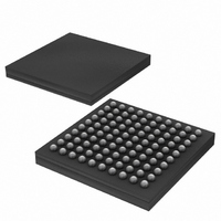
DS3170N+ Maxim Integrated Products, DS3170N+ Datasheet - Page 43

DS3170N+
Manufacturer Part Number
DS3170N+
Description
IC TXRX DS3/E3 100-CSBGA
Manufacturer
Maxim Integrated Products
Datasheet
1.DS3170.pdf
(230 pages)
Specifications of DS3170N+
Function
Single-Chip Transceiver
Interface
DS3, E3
Number Of Circuits
1
Voltage - Supply
3.135 V ~ 3.465 V
Current - Supply
120mA
Operating Temperature
-40°C ~ 85°C
Mounting Type
Surface Mount
Package / Case
100-LBGA
Includes
DS3 Framers, E3 Framers, HDLC Controller, On-Chip BERTs
Lead Free Status / RoHS Status
Lead free / RoHS Compliant
Power (watts)
-
- Current page: 43 of 230
- Download datasheet (3Mb)
Figure 8-16. DS3 Framed Mode Receive Serial Interface Pin Timing
Figure 8-17. E3 G.751 Framed Mode Receive Serial Interface Pin Timing
Figure 8-18. E3 G.832 Framed Mode Receive Serial Interface Pin Timing
8.3.4 Microprocessor Interface Functional Timing
8.3.4.1
NOTE: The transmit and receive order of the address and data bits are selected by the D[5]/SPI_SWAP pin. The
R/W (read/write) MSB bit and B (burst) LSB bit position is not effected by the D[5]/SPI_SWAP pin setting.
8.3.4.1.1
When CPHA = 0, CS may be de-asserted between accesses. An access is defined as one or two control bytes
followed by a data byte. CS cannot be de-asserted between the control bytes, or between the last control byte and
the data byte. When CPHA = 0, CS may also remain asserted between accesses. If it remains asserted and the
BURST bit is set, no additional control bytes are expected after the first control byte(s) and data are transferred. If
the BURST bit is set, the address will be incremented for each additional byte of data transferred until CS is de-
asserted. If CS remains asserted and the BURST bit is not set, a control byte(s) is expected following the data byte,
and the address for the next access will be received from that. Anytime CS is de-asserted, the BURST access is
terminated.
When CPHA = 1, CS may remain asserted for more than one access without being toggled high and then low
again between accesses. If the BURST bit is set, the address should increment and no additional control bytes are
DS3 RGCLK
E3 RGCLK
RCLKO or
RCLKO or
DS3 RSER
DS3 RDEN
E3 RGCLK
RCLKO or
E3 RSER
E3 RDEN
RSOFO
E3 RSER
E3 RDEN
RSOFO
RCLKI
RCLKI
RCLKI
RSOF
SPI Functional Timing Diagrams
SPI Transmission Format and CPHA Polarity
1
1
1
2
2
2
3
3
3
X1
4
4
4
5
5
5
6
6
FA1 11110110
6
FAS 1111010000
7
7
7
8
8
8
9
9
9
43 of 230
10
10
10
11
11
11
12
12
12
13
13
13
FA2 00101000
A
14
14
14
15
15
N
15
DS3170 DS3/E3 Single-Chip Transceiver
16
17
18
19
20
Related parts for DS3170N+
Image
Part Number
Description
Manufacturer
Datasheet
Request
R

Part Number:
Description:
IC TXRX DS3/E3 100-CSBGA
Manufacturer:
Maxim Integrated Products
Datasheet:

Part Number:
Description:
Network Controller & Processor ICs DS3-E3 Single-Chip T ransceiver T3-E3 Fra
Manufacturer:
Maxim Integrated Products
Datasheet:

Part Number:
Description:
MAX7528KCWPMaxim Integrated Products [CMOS Dual 8-Bit Buffered Multiplying DACs]
Manufacturer:
Maxim Integrated Products
Datasheet:

Part Number:
Description:
Single +5V, fully integrated, 1.25Gbps laser diode driver.
Manufacturer:
Maxim Integrated Products
Datasheet:

Part Number:
Description:
Single +5V, fully integrated, 155Mbps laser diode driver.
Manufacturer:
Maxim Integrated Products
Datasheet:

Part Number:
Description:
VRD11/VRD10, K8 Rev F 2/3/4-Phase PWM Controllers with Integrated Dual MOSFET Drivers
Manufacturer:
Maxim Integrated Products
Datasheet:

Part Number:
Description:
Highly Integrated Level 2 SMBus Battery Chargers
Manufacturer:
Maxim Integrated Products
Datasheet:

Part Number:
Description:
Current Monitor and Accumulator with Integrated Sense Resistor; ; Temperature Range: -40°C to +85°C
Manufacturer:
Maxim Integrated Products

Part Number:
Description:
TSSOP 14/A°/RS-485 Transceivers with Integrated 100O/120O Termination Resis
Manufacturer:
Maxim Integrated Products

Part Number:
Description:
TSSOP 14/A°/RS-485 Transceivers with Integrated 100O/120O Termination Resis
Manufacturer:
Maxim Integrated Products

Part Number:
Description:
QFN 16/A°/AC-DC and DC-DC Peak-Current-Mode Converters with Integrated Step
Manufacturer:
Maxim Integrated Products

Part Number:
Description:
TDFN/A/65V, 1A, 600KHZ, SYNCHRONOUS STEP-DOWN REGULATOR WITH INTEGRATED SWI
Manufacturer:
Maxim Integrated Products

Part Number:
Description:
Integrated Temperature Controller f
Manufacturer:
Maxim Integrated Products

Part Number:
Description:
SOT23-6/I°/45MHz to 650MHz, Integrated IF VCOs with Differential Output
Manufacturer:
Maxim Integrated Products

Part Number:
Description:
SOT23-6/I°/45MHz to 650MHz, Integrated IF VCOs with Differential Output
Manufacturer:
Maxim Integrated Products


